BA7230LS データシートの表示(PDF) - ROHM Semiconductor
部品番号
コンポーネント説明
メーカー
BA7230LS Datasheet PDF : 8 Pages
| |||
Multimedia ICs
BA7230LS
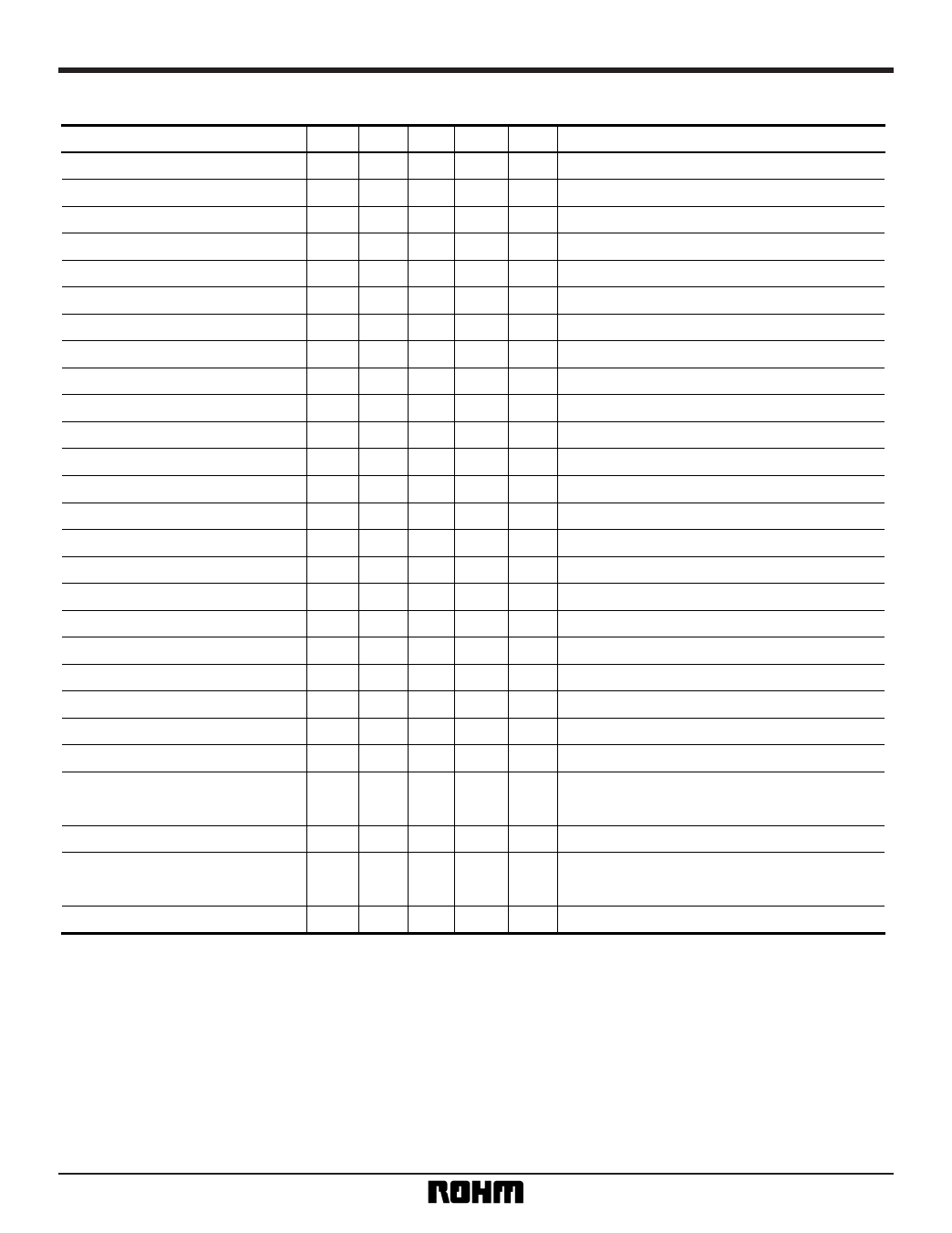
•Electrical characteristics (unless otherwise noted, Ta = 25°C, VCC = 5.0V)
Parameter
Symbol Min. Typ.
Quiescent current
IQ
— 38
Video output level
VOV 1.7 2.2
Half down level change
GVH – 3 – 5
DC offset
VOF
—
50
Crosstalk
CT — – 46
ER-EY output level
VR-Y 0.3 0.42
EB-EY output level
VB-Y 0.2 0.31
YOUT output level
VY 1.0 1.4
Ys switching delay time
TD
—
60
SYNC output level
VOS 0.4 0.65
Burst output level
VOB 0.25 0.46
Composite output level
VOY 1.7 2.2
R-Y modulation gain
GR-Y
9
11
B-Y modulation gain
GB-Y
9
11
(R-Y) / (B-Y) modulation gain differential GR-B — —
(R-Y) / (B-Y) orthogonal phase shift
∆R – 6
—
(R - Y) ·Burst orthogonal phase shift
∆B – 6
—
Carrier leak
LSC
—
30
APC capture range
fCAP ± 100 —
Carrier phase range
φSC ± 30 ± 45
Video frequency characteristic
fV
4.5
6
Video output DG
DG — ± 3.5
Video output DP
DP — ± 2.5
Max.
54
2.6
–7
160
– 40
0.55
0.42
1.8
—
0.9
0.8
2.6
13
13
2
6
6
70
—
—
—
—
—
Unit
Conditions
mA
—
VP-P VIDEO IN = 1VP-P
dB
—
mVP-P VIDEO IN = 1VP-P
dB VIDEO IN = 1VP-P
VP-P VR = 0.7VP-P
VP-P VB = 0.7VP-P
VP-P VR = VG = VB = 0.7VP-P
ns
—
VP-P
—
VP-P RE = 1.8kΩ
VP-P YIN = 0.7VP-P
dB R - YIN = 0.3VP-P
dB B - YIN = 0.2VP-P
dB Difference between above gains
deg
—
deg
—
mVP-P VOUT = 2VP-P
Hz Burst = 0.1VP-P, 2.8µS
deg Superimposition
MHz – 3dB when f = 100kHz
% VIDEO IN = 1VP-P
deg VIDEO IN = 1VP-P
Input impedance (SY, BF, PC, HD)
ZT
8 15 — kΩ
—
Input impedance (Ys)
ZTY
3
7.5 —
kΩ
—
Threshold level (SY, BF, PC, HD)
VT 0.9 2.0 2.8
V
—
Threshold level (Ys)
VTY 0.5 1.1 1.8
V
—
3
Share Link: 