RC1117DT データシートの表示(PDF) - Fairchild Semiconductor
部品番号
コンポーネント説明
メーカー
RC1117DT Datasheet PDF : 9 Pages
| |||
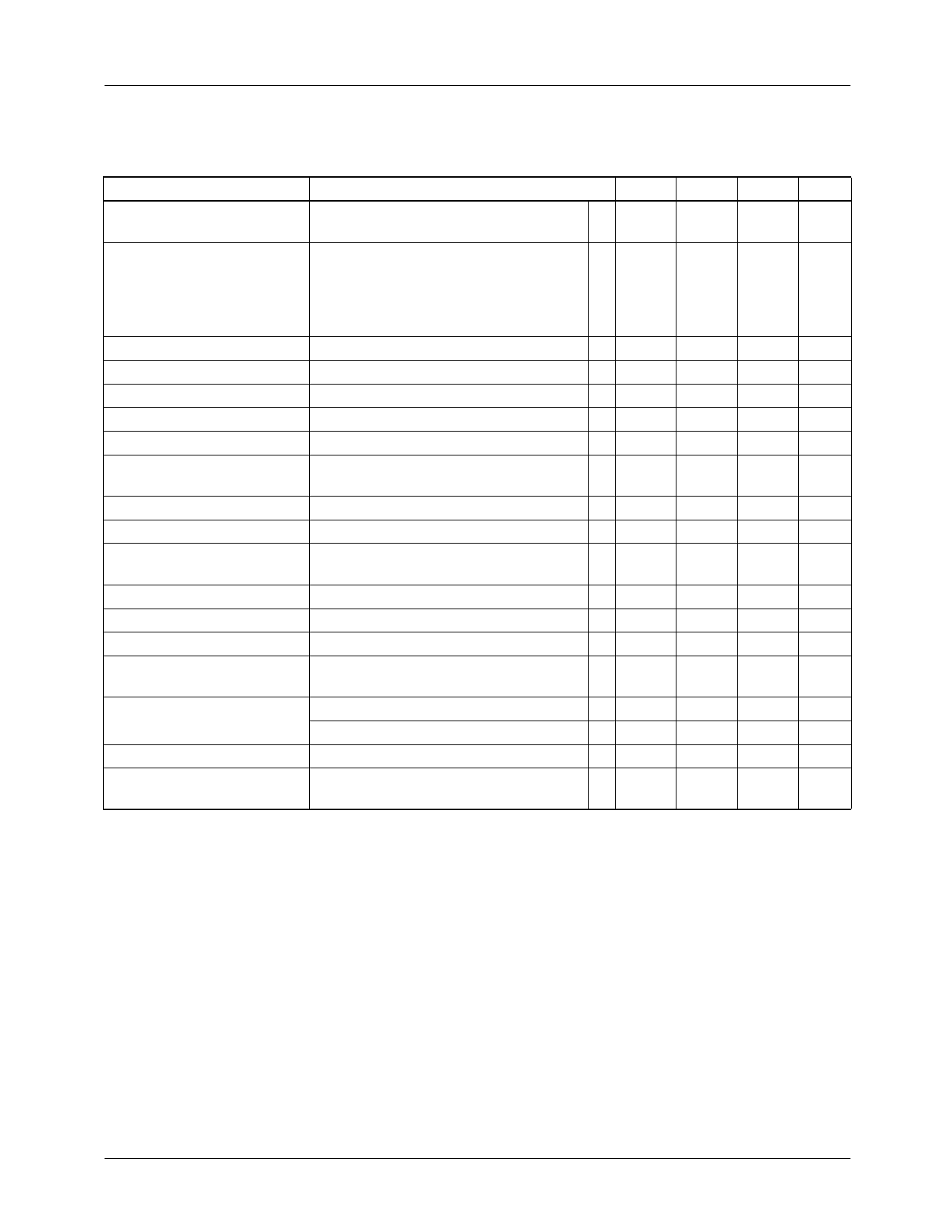
RC1117
PRODUCT SPECIFICATION
Electrical Characteristics
Operating Conditions: VIN ≤ 7V, TJ = 25°C unless otherwise specified.
The • denotes specifications which apply over the specified operating temperature range.
Parameter
Conditions
Min. Typ. Max. Units
Reference Voltage, VREF3
1.5V ≤ (VIN - VOUT) ≤ 5.75V,
10mA ≤ IOUT ≤ 1A
• 1.225 1.250 1.275 V
(-2%)
(+2%)
Output Voltage
Line Regulation1,2
Load Regulation1,2
10mA ≤ IOUT ≤ 1A
RC1117-2.5, 4V ≤ VIN ≤ 7V
RC1117-2.85, 4.35V ≤ VIN ≤ 7V
RC1117-3.3, 4.8V ≤ VIN ≤ 7V
RC1117-5, 6.5V ≤ VIN ≤ 7V
• 2.450 2.5 2.550 V
• 2.793 2.85 2.907 V
• 3.234 3.3 3.366 V
• 4.900 5.0 5.100 V
(VOUT + 1.5V) ≤ VIN ≤ 7V, IOUT = 10mA •
0.005 0.2
%
(VIN – VOUT) = 2V, 10mA ≤ IOUT ≤ 1A
•
0.05 0.5
%
Dropout Voltage
∆VREF = 1%, IOUT = 1A
•
1.100 1.200 V
Current Limit
Adjust Pin Current, IAdj3
Adjust Pin Current Change3
(VIN – VOUT) = 2V
1.5V ≤ (VIN – VOUT) ≤ 5.75,
10mA ≤ IOUT ≤ 1A
• 1.1
1.5
A
•
35
120 µA
•
0.2
5
µA
Minimum Load Current
1.5V ≤ (VIN – VOUT) ≤ 5.75
• 10
mA
Quiescent Current
VIN = VOUT + 1.25V
•
4
13 mA
Ripple Rejection
f = 120Hz, COUT = 22µF Tantalum,
60
72
dB
(VIN – VOUT) = 3V, IOUT = 1A
Thermal Regulation
TA = 25°C, 30ms pulse
0.004 0.02 %/W
Temperature Stability
•
0.5
%
Long-Term Stability
RMS Output Noise
(% of VOUT)
Thermal Resistance, Junction
to Case
TA = 125°C, 1000hrs.
TA = 25°C, 10Hz ≤ f ≤ 10kHz
SOT-223
TO-252, TO-263
0.03
0.003
15
3
1.0
%
%
°C/W
°C/W
Thermal Shutdown
Junction Temperature
155
°C
Thermal Shutdown
Hysteresis
10
°C
Notes:
1. See thermal regulation specifications for changes in output voltage due to heating effects. Load and line regulation are
measured at a constant junction temperature by low duty cycle pulse testing.
2. Line and load regulation are guaranteed up to the maximum power dissipation (18W). Power dissipation is determined by
input/output differential and the output current. Guaranteed maximum output power will not be available over the full input/
output voltage range.
3. RC1117 only.
REV. 1.3.2 10/16/03
3
Share Link: 