MAC7100 データシートの表示(PDF) - Motorola => Freescale
部品番号
コンポーネント説明
メーカー
MAC7100 Datasheet PDF : 48 Pages
| |||
Freescale Semiconductor, Inc.
Electrical Characteristics
3.9 External Bus Timing Specifications
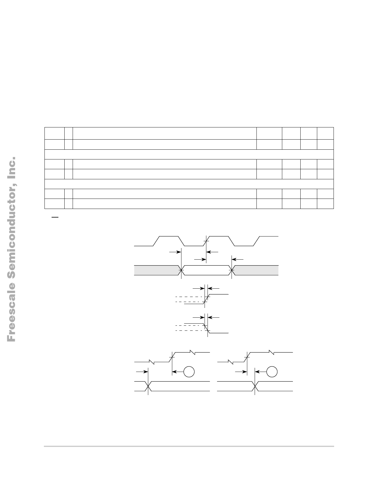
Table 22 lists processor bus input timings, which are shown in Figure 6, Figure 7 and Figure 8.
NOTE
All processor bus timings are synchronous; that is, input setup/hold and
output delay with respect to the rising edge of a reference clock. The
reference clock is the CLKOUT output.
All other timing relationships can be derived from these values.
Table 22. External Bus Input Timing Specifications
Num C
Rating 1
Symbol Min Max Unit
L1
CLKOUT
Control Inputs
L2a
Control input valid to CLKOUT high 2
L3a
CLKOUT high to control inputs invalid 2
Data Inputs
tCYC
23 — ns
tCVCH 13 — ns
tCHCII
0
— ns
L4
Data input (DATA[15:0]) valid to CLKOUT high
tDIVCH
9
L5
CLKOUT high to data input (DATA[15:0]) invalid
tCHDII
0
1 Timing specifications have been indicated taking into account the full drive strength for the pads.
2 TA pins are being referred to as control inputs.
— ns
— ns
CLKOUT(45MHz)
Input Setup & Hold
Input Rise Time
Input Fall Time
tSETUP
Invalid
1.5 V
1.5 V Valid 1.5 V
tHOLD
Invalid
VH = VIH
VL = VIL
VH = VIH
VL = VIL
tRISE = 1.5 ns
tFALL = 1.5 ns
CLKOUT
L4
L5
Inputs
Figure 6. General Input Timing Requirements
19
MAC7100 Microcontroller Family Hardware Specifications
MOTOROLA
PRELIMINARY—SUBJECT TO CHANGE WITHOUT NOTICE
For More Information On This Product,
Go to: www.freescale.com
Share Link: 