ATA6613 データシートの表示(PDF) - Atmel Corporation
部品番号
コンポーネント説明
メーカー
ATA6613 Datasheet PDF : 364 Pages
| |||
ATA6612/ATA6613
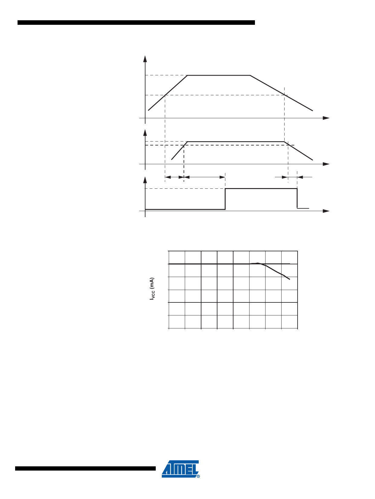
Figure 3-7. VCC Voltage Regulator: Ramp Up and Undervoltage Detection
VS
12V
5.5V/3.8V
VCC
5V/3.3V
Vthun
NRES
5V/3.3V
TVCC
TReset
t
Tres_f t
t
Figure 3-8.
Power Dissipation: Safe Operating Area versus VCC Output Current and Supply
Voltage VS at Different Ambient Temperatures Due to Rthja = 35 K/W
60
Tamb = 105°C
50
Tamb = 125°C
40
30
20
10
0
3
5
7
9
11
13
15
17
19
VS (V)
For programming purposes of the microcontroller it is potentially necessary to supply the VCC
output via an external power supply while the VS Pin of the system basis chip is disconnected.
This behavior is no problem for the system basis chip.
For programming purposes of the microcontroller it is potentially neccessary to supply the VCC
output via an external power supply while the VS Pin of the system basis chip is disconnected.
This behavior is no problem for the system basis chip.
17
9111G–AUTO–05/10
Share Link: 