TSA5522 データシートの表示(PDF) - Philips Electronics
部品番号
コンポーネント説明
メーカー
TSA5522 Datasheet PDF : 20 Pages
| |||
Philips Semiconductors
1.4 GHz I2C-bus controlled synthesizer
Product specification
TSA5522
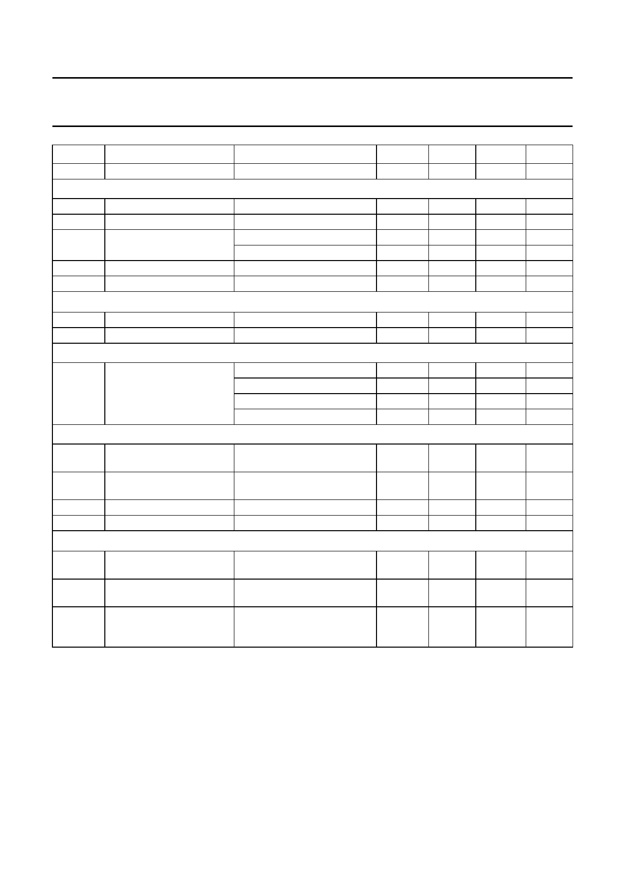
SYMBOL
PARAMETER
CONDITIONS
MIN.
TYP.
MAX
UNIT
IIL(AS)
LOW level input current
SCL and SDA inputs
VAS = 0 V
−50
−
−
µA
VIL
LOW level input voltage
−
VIH
HIGH level input voltage
3.0
IIH
HIGH level input current VIH = 5.5 V; VCC1 = 0 V
−
VIH = 5.5 V; VCC1 = 5.5 V
−
IIL
LOW level input current
VIL = 0 V; VCC1 = 5.5 V
−10
fclk
input clock frequency
−
SDA output (I2C bus mode)
IILO
output leakage current
VO = 5.5 V
−
Vo
output voltage
Isink = 3 mA
−
BS output (M/O band selection)
−
1.5
V
−
5.5
V
−
10
µA
−
10
µA
−
−
µA
100
400
kHz
−
10
µA
−
0.4
µA
Vo(BS)
output voltage
Charge-pump output CP
band A; Isource = 20 µA
band B; Isource = 20 µA
band C; Isource = 20 µA
band C; Isource = 50 µA
−
0.36VCC1
0.7VCC1
3.1
0.25
0.4VCC1
0.8VCC1
−
0.5
V
0.43VCC1 V
0.9VCC1 V
−
V
IICPH HIGH charge pump current CP = 1
−
(absolute value)
IICPL LOW charge pump current CP = 0
−
(absolute value)
Vo(CP)
output voltage
in-lock; Tamb = +25 °C
−
ILI(off)
off-state leakage current T2 = 0; T1 = 1
−5
Tuning voltage output Vtune
ILO(off)
leakage current when
OS = 1; Vtune = 33 V
−
switched-off
Vo
Vripple(p-p)
output voltage when the
loop is closed
acceptable ripple voltage
on VCC1 (peak-to-peak
value)
OS = 0; T2 = 0; T1 = 0; T0 = 1; 0.4
RL = 27 k Ω; Vtune = 33 V
fripple = 300 Hz to 300 kHz
−
250
−
µA
50
−
µA
1.95
−
V
1
15
nA
−
10
µA
−
32.6
V
−
30
mV
Notes
1. A single PNP band switch buffer is ON.
2. P4, P5 and P7 I/O ports are not available in 16-pin package. In 20-pin package, when a port is active, the collector
voltage must not exceed 6 V.
3. A single NPN open-collector output is ON.
1996 Jan 23
10
Share Link: 