LA4663 データシートの表示(PDF) - SANYO -> Panasonic
部品番号
コンポーネント説明
メーカー
LA4663 Datasheet PDF : 10 Pages
| |||
LA4663
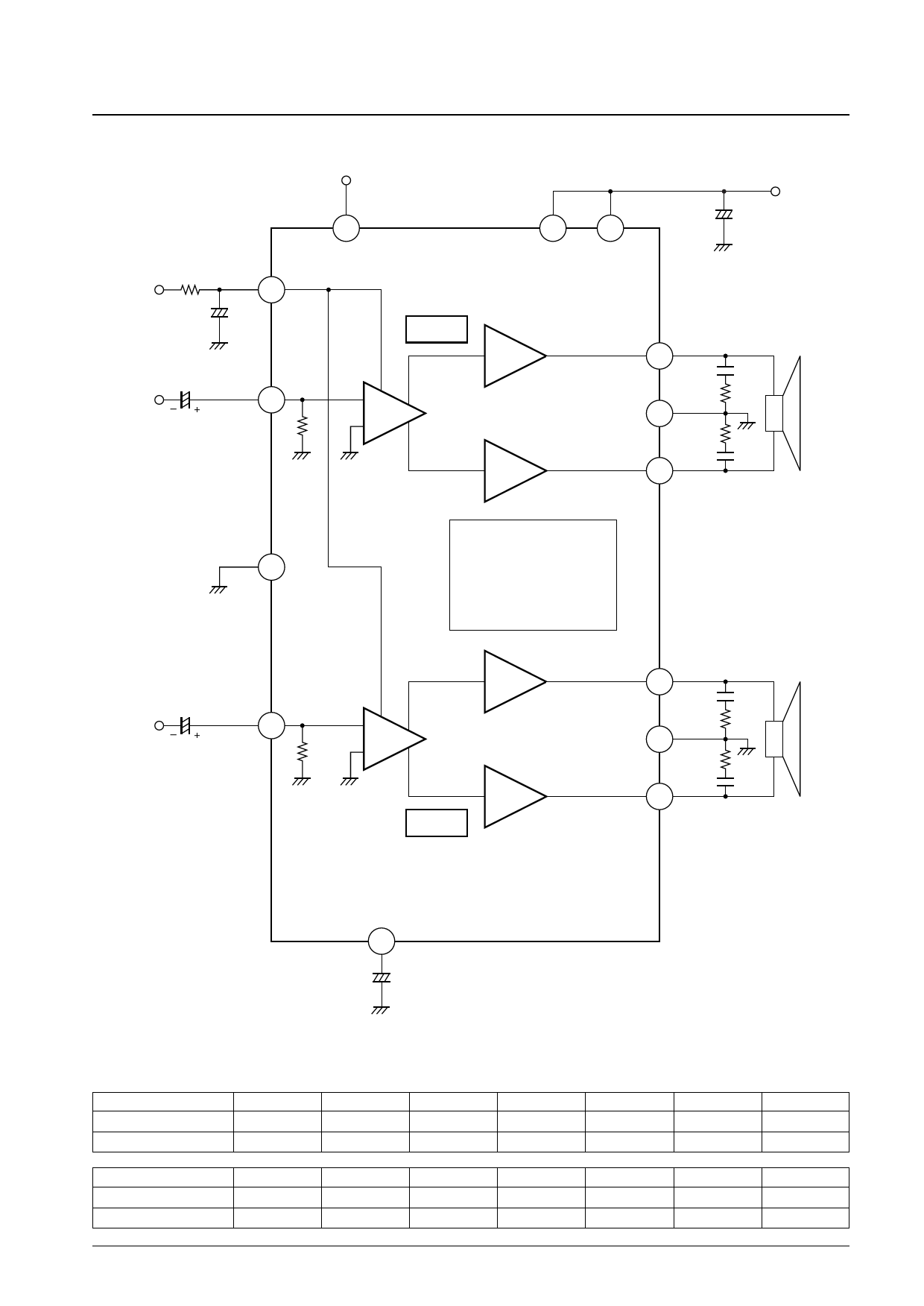
Equivalent Circuit Block Diagram
+5 V
R1
22 kΩ
SIGNAL
MUTE
6
+5 V
+ C4
– 10 µF
10 V
C1
4.7 µF
10 V
IN1
2
5
STAND BY
7
VCC1
CH 1
+
Output amplifier
–
Ri =
20 kΩ Input amplifier
8
VCC2
+OUT1
14
PWR
GND1
13
12
–OUT1
VCC
+ C5
– 2200 µF
25 V
C6
0.1 µF
RL = 4 to 8 Ω
**
R2
2.2 Ω
R3
2.2 Ω
**
C7
0.1 µF
PRE
GND
3
VCC/ground shorting protection
circuit
Load shorting protection circuit
Thermal protection circuit
— Protection circuits —
**
Polyester film capacitors
C2
4.7 µF
10 V
Input amplifier
IN2
4
Ri =
20 kΩ
+
Output amplifier
–
CH 2
+OUT2
9
PWR
GND2
10
11
–OUT2
C8
0.1 µF
RL = 4 to 8 Ω
**
R4
2.2 Ω
R5
2.2 Ω
**
C9
0.1 µF
Ripple Filter/
Starting Time
1
+ C3
– 47 µF
25 V
A10630
Pin Voltages at VCC = 15 V, with 5 V applied to the STBY pin (pin 5), using a digital volt meter.
Pin No.
Pin
Pin voltage (V)
1
RF
14.32
2
3
4
5
6
IN1
PRE-GND
IN2
STAND-BY
MUTE
3m
0
3m
5
21m
7
VCC1
15
Pin No.
Pin
Pin voltage (V)
8
VCC2
15
9
+OUT2
6.84
10
PWR-GND2
0
11
–OUT2
6.84
12
–OUT1
6.84
13
PWR-GND1
0
14
+OUT1
6.84
No. 5905-5/10
Share Link: 