HMP8156 データシートの表示(PDF) - Intersil
部品番号
コンポーネント説明
メーカー
HMP8156 Datasheet PDF : 33 Pages
| |||
HMP8156
The analog RGB outputs have a range of 0.3-1.0V with no
blanking pedestal. Composite sync information (0.0-0.3V)
may be optionally added to the green output. Closed cap-
tioning data is not included on the RGB outputs.
The HMP8156 also generates composite video when in
RGB output mode. The analog composite video is output
onto the NTSC/PAL 1 pin. Red information is output onto the
NTSC/PAL 2 pin, blue information is output onto the C pin,
and green information is output onto the Y pin. All four out-
puts are time aligned.
Power Down Mode
When the power down mode is enabled, all of the DACs are
powered down (forcing their outputs to zero) and most of the
internal clocks are stopped. The host processor may still
read from and write to the internal control registers.
Host Interfaces
Reset
The HMP8156 resets to its default operating mode on power
up, when the reset pin is asserted for at least four CLK
cycles, or when the software reset bit of the host control reg-
ister is set. During the reset cycle, the encoder returns its
internal registers to their reset state and deactivates the I2C
interface.
I2C Interface
The HMP8156 provides a standard I2C interface and sup-
ports fast-mode (up to 400 KBPS) transfers. The device acts
as a slave for receiving and transmitting data only. It will not
respond to general calls or initiate a transfer. The encoder’s
slave address is either 0100 000xB when the SA input pin is
iloswthoerI20C10r0ea0d01flxaBg.w) hen it is high. (The ‘x’ bit in the address
The I2C interface consists of the SDA and SCL pins. When
the interface is not active, SCL and SDA must be pulled high
using external 4-6kΩ pull-up resistors. The I2C clock and
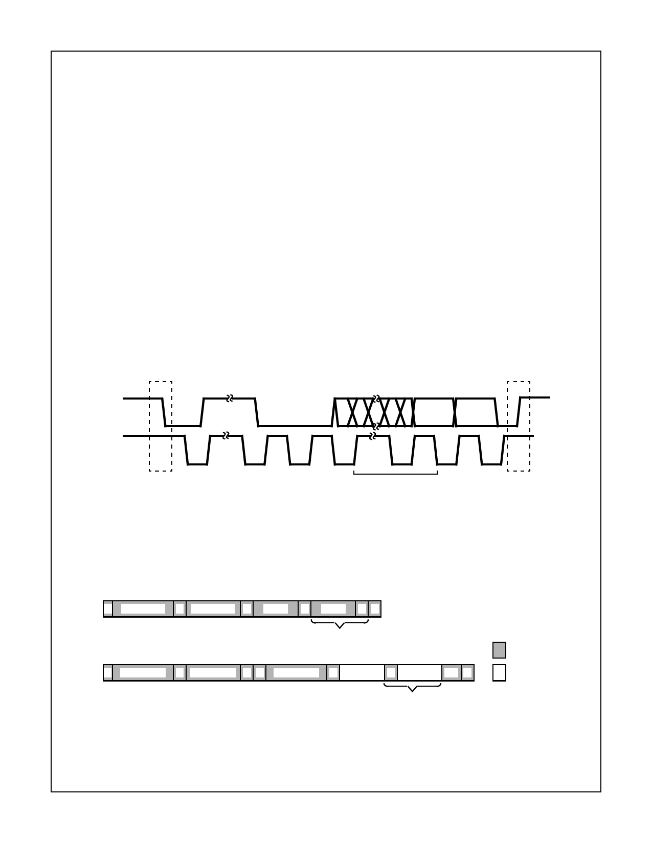
data timing is shown in Figures 15 and 16.
SDA
SCL
S
1-7
8
START
ADDRESS
R/W
CONDITION
9
ACK
1-7
8
DATA
FIGURE 15. I2C SERIAL TIMING FLOW
9
ACK
P
STOP
CONDITION
DATA WRITE
0100 000 OR
0100 0010
S CHIP ADDR
0x40 OR
0x42
DATA READ
A SUB ADDR
A DATA A DATA A P
REGISTER
POINTED
TO BY
SUBADDR
OPTIONAL FRAME
MAY BE REPEATED
n TIMES
S CHIP ADDR A SUB ADDR A S CHIP ADDR A DATA A DATA NA P
0x41 OR
0x43
REGISTER
POINTED
TO BY
SUBADDR
OPTIONAL FRAME
MAY BE REPEATED
n TIMES
FIGURE 16. REGISTER WRITE PROGRAMMING FLOW
S = START CYCLE
P = STOP CYCLE
A = ACKNOWLEDGE
NA = NO ACKNOWLEDGE
FROM MASTER
FROM HMP8156
15
Share Link: 