ST95P04 データシートの表示(PDF) - STMicroelectronics
部品番号
コンポーネント説明
メーカー
ST95P04 Datasheet PDF : 16 Pages
| |||
ST95P04
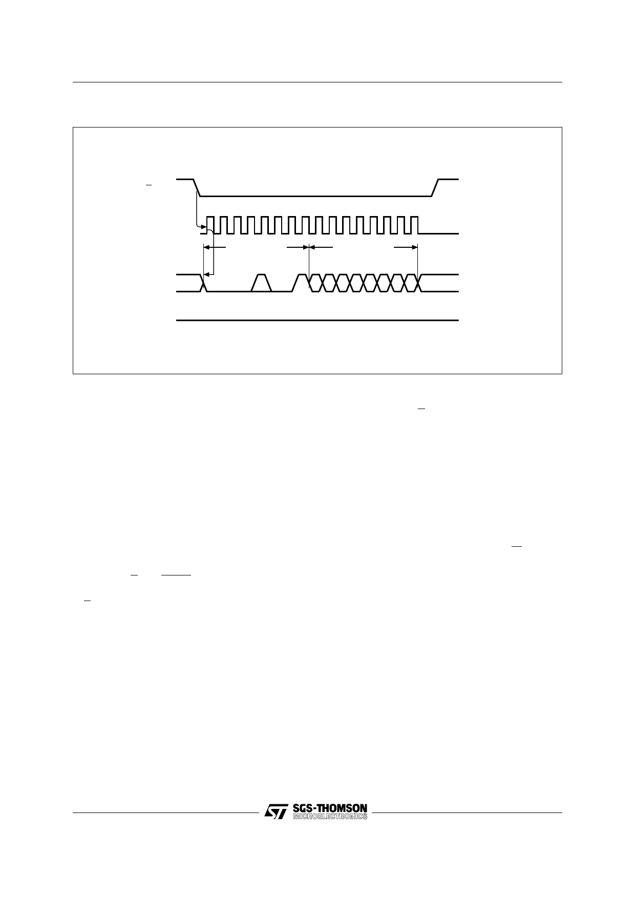
Figure 13. WRSR: Write Status Register Sequence
S
0 1 2 3 4 5 6 7 8 9 10 11 12 13 14 15
C
INSTRUCTION
STATUS REG.
D
HIGH IMPEDANCE
Q
AI01434
POWER ON STATE
After a Power up the ST95P04 is in the following
state:
– The device is in the low power standby state.
– The chip is deselected.
– The chip is not in hold condition.
– The write enable latch is reset.
– BP1 and BP0 are unchanged (non-volatile
bits).
DATA PROTECTION AND PROTOCOL SAFETY
– All inputs are protected against noise, see Ta-
ble 3.
– Non valid S and HOLD transitions are not
taken into account.
– S must come high at the proper clock count in
order to start a non-volatile write cycle (in the
memory array or in the cycle status register).
The Chip Select S must rise during the clock
pulse following the introduction of a multiple of
8 bits.
– Access to the memory array during non-vola-
tile programming cycle is cancelled and the
chip is automatically deselected; however, the
programming cycle continues.
– After either of the following operations
(WREN, WRDI, RDSR) is completed, the chip
enters a wait state and waits for a deselect.
– The write enable latch is reset upon power-up.
– The write enable latch is reset when W is
brought low.
INITIAL DELIVERY STATE
The device is delivered with the memory array in a
fully erased state (all data set at all "1’s" or FFh).
The block protect bits are initialized to 00.
12/16
Share Link: 