ICX282 データシートの表示(PDF) - Sony Semiconductor
部品番号
コンポーネント説明
メーカー
ICX282 Datasheet PDF : 51 Pages
| |||
CXD2498R
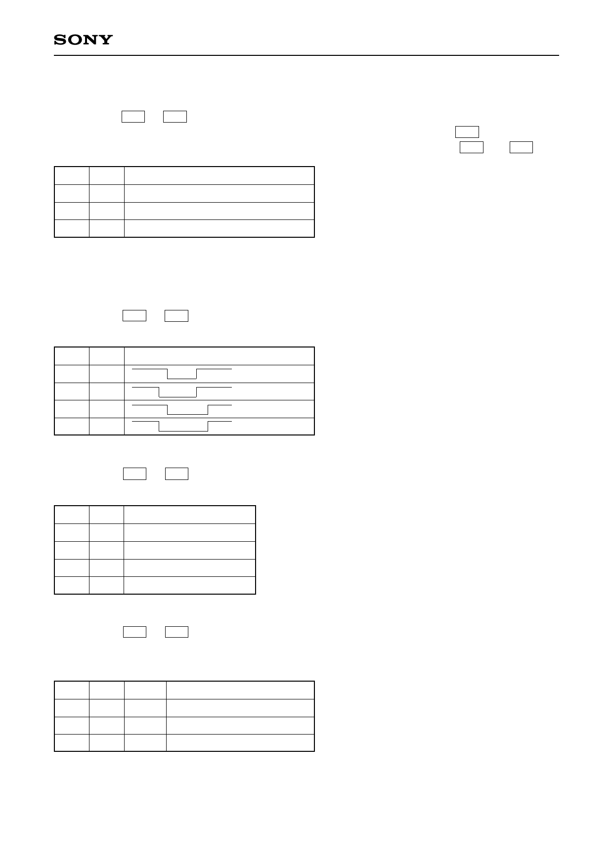
Detailed Description of Each Data
Shared data: D08 to D09 CTG [Category]
Of the data provided to the CXD2498R by the serial interface, the CXD2498R loads D10 and subsequent
data to each data register as shown in the table below according to the combination of D08 and D09 .
D09 D08
Description of operation
0
0 Loading to control data register
0
1 Loading to shutter data register
1
X Test mode
Note that the CXD2498R can apply these categories consecutively within the same vertical period. However,
care should be taken as the data is overwritten if the same category is applied.
Control data: D34 to D35 PTOB [OBCLP waveform pattern]
This specifies the OBCLP waveform pattern. The default is “Normal”. See the Timing Charts for details.
D35 D34
0
0
0
1
1
0
1
1
Waveform pattern
(Normal)
(Rearward)
(Forward)
(Wide)
Control data: D36 to D37 LDAD [ADCLK logic phase]
This indicates the ADCLK logic phase adjustment data. The default is 90° relative to MCKO.
D37 D36 Degree of adjustment (°)
0
0
0
0
1
90
1
0
180
1
1
270
Control data: D38 to D39 STB [Standby]
The operating mode is switched as follows. However, the standby bits are loaded to the CXD2498R and control
is applied immediately at the rising edge of SEN.
D39 D38 Symbol
Operating mode
X
0 CAM Normal operating mode
0
1 SLP Sleep mode
1
1 STB Standby mode
See the Pin Status Table for the pin status in each mode.
– 18 –
Share Link: 