NJU6624C データシートの表示(PDF) - Japan Radio Corporation
部品番号
コンポーネント説明
メーカー
NJU6624C
Japan Radio Corporation

NJU6624C Datasheet PDF : 27 Pages
| |||
NJU6624C
(m)Write Data to CG, DD or MK RAM
By the execution of this instruction, the binary 8-bit data (A7 to A0) are written into the DD RAM, and the binary 5-
bit data (A4 to A0) are written into the CG or MK RAM. The selection of RAM is determined by the previous in-
struction. After this instruction execution, the address increment (+1) or decrement(-1) is performed automatically
according to the entry mode set. And the display shift is also executed according to the previous entry mode set.
However, the data in MK RAM (1C)H and (1D)H are not displayed, bat the automatic address increment is per-
formed. And the display is not changed by the data written into MK RAM (1C)H and (1D)H
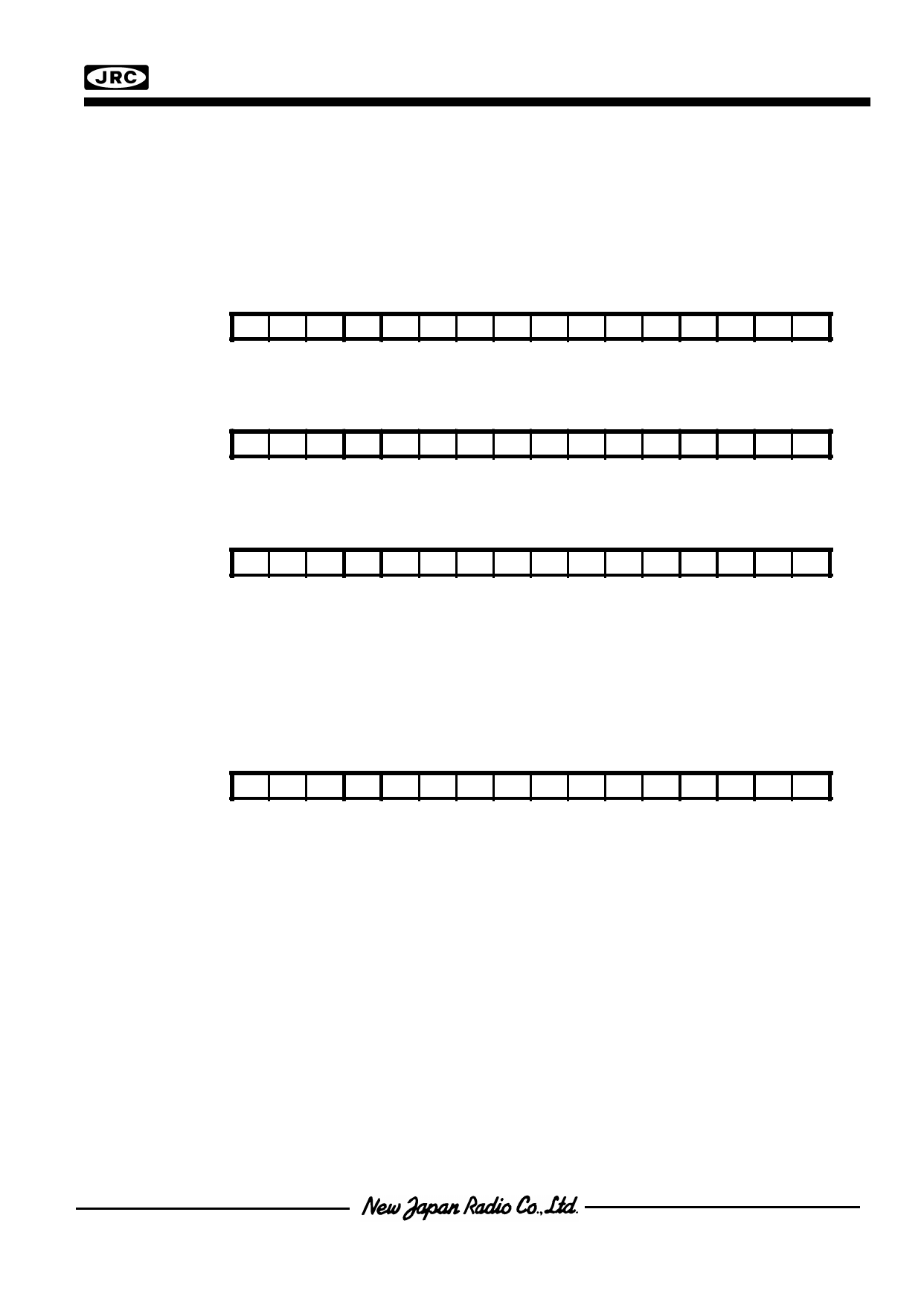
-Write Data to DD RAM
D15 D14 D13 D12 D11 D10 D9 D8 D7 D6 D5 D4 D3 D2 D1 D0
Code 1 0 0 1 1 0 0 0 DD7 DD6 DD5 DD4 DD3 DD2 DD1 DD0
-Write Data to MK RAM
D15 D14 D13 D12 D11 D10 D9 D8 D7 D6 D5 D4 D3 D2 D1 D0
Code 1 0 0 1 0 0 0 0 * * * DM4 DM3 DM2 DM1 DM0
-Write Data to CG RAM
D15 D14 D13 D12 D11 D10 D9 D8 D7 D6 D5 D4 D3 D2 D1 D0
Code 1 0 0 1 0 0 0 0 * * * DC4 DC3 DC2 DC1 DC0
(n)Read Data Key
D15 D14 D13 D12 D11 D10 D9 D8 D7 D6 D5 D4 D3 D2 D1 D0
Code 1 0 1 0 0 1 1 1 KL3 KL2 KL1 KL0 0 KH2 KH1 KH0
Read data key is a instruction for data reading out of keyscan. However, the bit 8 to 15 are input data. After this 8-
bit data were input, the operation change to output from input at the falling edge of 8th SCK clock.
Share Link: