MCP1256 データシートの表示(PDF) - Microchip Technology
部品番号
コンポーネント説明
メーカー
MCP1256
Microchip Technology

MCP1256 Datasheet PDF : 24 Pages
| |||
MCP1256/7/8/9
4.0 DEVICE OVERVIEW
The MCP1256/7/8/9 devices are positive regulated
charge pumps that accept an input voltage from +1.8V
to +3.6V and convert it to a regulated 3.3V output volt-
age. The MCP1256/7/8/9 provide a low-cost, compact
and simple solution for step-up DC/DC conversions,
primarily in battery applications, that do not want to use
switching regulator solutions because of EMI noise and
inductor size.
The MCP1256/7/8/9 are designed to offer the highest
possible efficiency under common operating condi-
tions, i.e. VIN = 2.4V or 2.8V, VOUT = 3.3V,
IOUT = 100 mA. A fixed switching frequency, 650 kHz
typically, allows for easy external filtering.
The MCP1256/7 provide a unique SLEEP mode
feature which reduces the current drawn from the input
supply while maintaining a regulated bias on external
peripherals. SLEEP mode can substantially increase
battery run-time in portable applications.
The MCP1258/9 provide a unique BYPASS mode
feature which virtually eliminates the current drawn
from the input supply by the device while maintaining
an unregulated bias on external peripherals. BYPASS
connects the input supply voltage to the output. All
remaining functions of the device are shutdown.
BYPASS mode can substantially increase battery run-
time in portable applications.
The devices supply up to 100 mA of output current for
input voltages, VIN, greater than or equal to 2.2V. The
devices are available in small 10-Pin MSOP or DFN
packages with an operating junction temperature range
of -40°C to +125°C.
4.1 Theory of Operation
The MCP1256/7/8/9 devices employ a switched capac-
itor charge pump to boost an input supply, VIN, to a reg-
ulated 3.3V output voltage. Refering to the Functional
Block Diagram, the devices perform conversion and
regulation in two phases: charge and transfer. When
the devices are not in shutdown, SLEEP or BYPASS,
the two phases are continuously cycled through.
Charge transfers charge from the input supply to the
flying capacitors, C1 and C2, connected to pins C1+,
C1-, C2+ and C2-, respectively. During this phase,
switches S4 and S6 are closed. Switch S2 controls the
amount of charge transferred to the flying capacitors.
The amount of charge is determined by a sample and
hold error amplifier with feedback from the output
voltage at the beginning of the phase.
Once the first phase (charge) is complete, transfer is
initiated. The second phase transfers the energy from
the flying capacitors to the output. The MCP1256/7/8/9
devices autonomously switch between 1.5x mode and
2x mode. This determines whether the flying capacitors
are placed in parallel (1.5x mode), or remain in series
DS21989A-page 12
(2x mode), when the energy is transferred to the out-
put. The transfer mode determines which switches are
closed for the transfer.
Both phases occur in one clock period of the internal
oscillator. When the second phase (transfer) has been
completed, the cycle repeats.
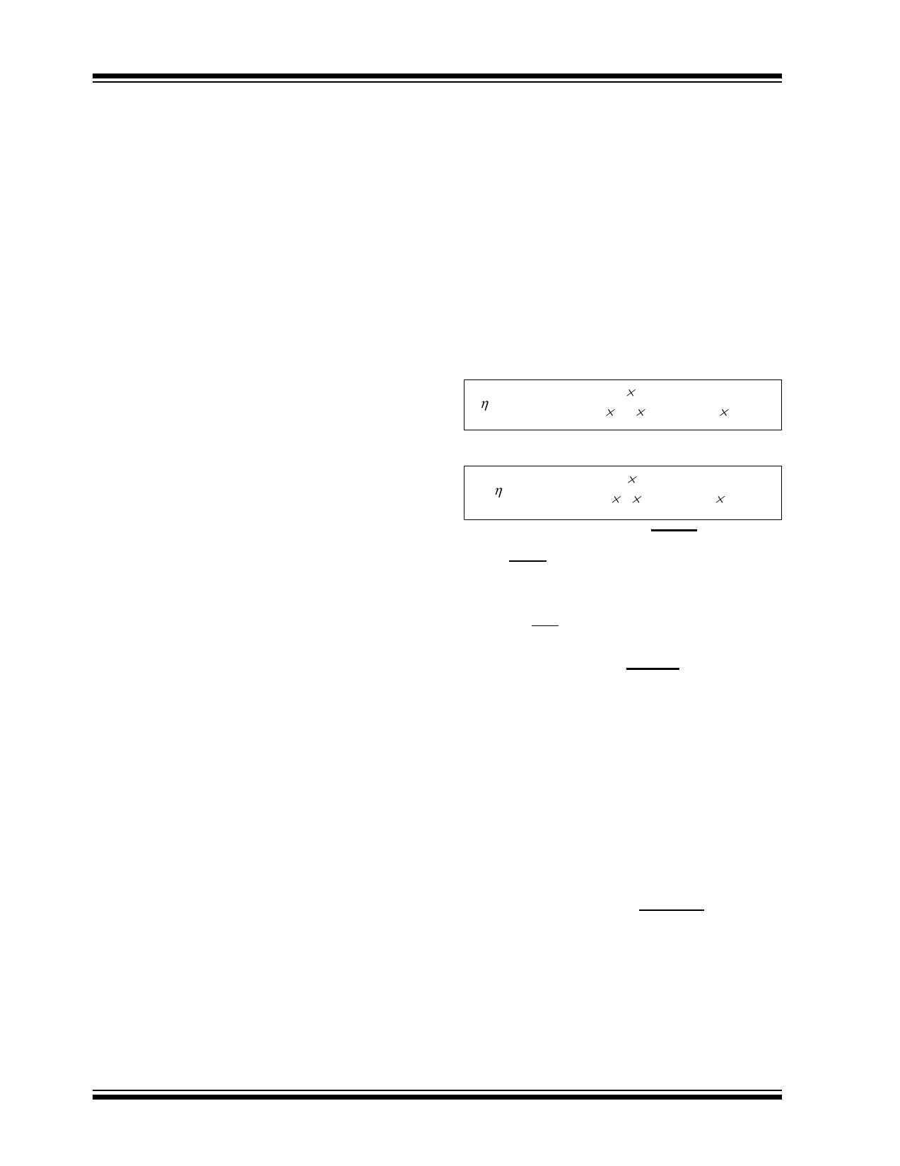
4.2 Power Efficiency
The power efficiency, η, is determined by the mode of
operation, 1.5x mode or 2x mode. Equation 4-1 and
Equation 4-2 are used to approximate the power effi-
ciency with any significant amount of output current. At
light loads, the device quiescent current must be taken
into consideration.
EQUATION 4-1:
η1.5x
=
P----O----U----T-
PIN
=
V----I-V-N---O--×--U---1T---.-5×-----×I--O---I-U-O---T-U---T-
=
V----I-V-N---O--×-U----1T---.-5--
EQUATION 4-2:
η2x
=
P----O----U----T-
PIN
=
V---V-I--N-O---U-×---T--2--×--×---I--IO--O--U--U--T--T-
=
V---V-I--N-O---U-×---T--2-
4.3 Shutdown Mode (SHDN)
Driving SHDN low places the MCP1256/7/8/9 in a low-
power Shutdown mode. This disables the charge-pump
switches, oscillator and control logic, reducing the
quiescent current to 0.25 μA (typical). The PGOOD
output and LBO are in a high impedance state during
shutdown.
4.4 SLEEP Mode (SLEEP)
The MCP1256/7 provide a unique SLEEP mode fea-
ture. SLEEP mode reduces the current drawn from the
input supply while maintaining a regulated bias on
external peripherals. SLEEP mode can substantially
increase battery run-time in portable applications.
The regulation control is referred to as a bang-bang
control due to the output being regulated around a fixed
reference with some hysteresis. As a result, some
amount of peak-to-peak ripple will be observed at the
output independent of load current. The frequency of
the output ripple, however, will be influenced heavily by
the load current and output capacitance.
4.5 BYPASS Mode (BYPASS)
The MCP1258/9 provide a unique BYPASS mode fea-
ture which virtually eliminates the current drawn from
the input supply by the device, while maintaining an
unregulated bias on external peripherals. BYPASS
connects the input supply voltage to the output. All
remaining functions of the device are shutdown.
BYPASS mode can substantially increase battery run-
time in portable applications.
© 2006 Microchip Technology Inc.
Share Link: