CM1631(2011) データシートの表示(PDF) - ON Semiconductor
部品番号
コンポーネント説明
メーカー
CM1631 Datasheet PDF : 16 Pages
| |||
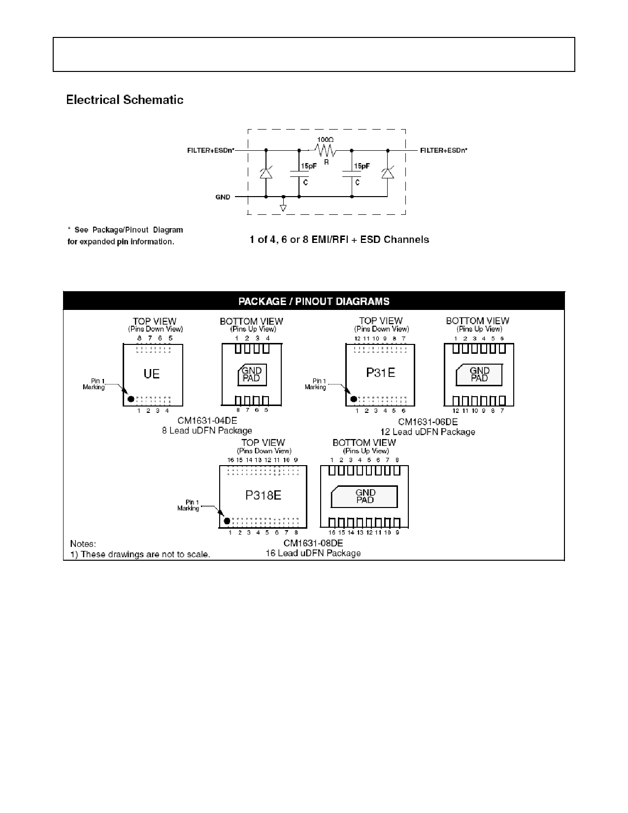
Top View
(Pins Down View)
8765
CM1631
PACKAGE / PINOUT DIAGRAMS
Bottom View
(Pins Up View)
1234
Top View
(Pins Down View)
12 11 10 9 8 7
Bottom View
(Pins Up View)
123456
Pin 1
UE
Marking
GND
PAD
Pin 1
Marking
P31E
GND
PAD
1234
8765
CM1631−04DE
8 Lead UDFN Package
Top View
(Pins Down View)
16 15 1413 12 11 10 9
123456
12 11 10 9 8 7
CM1631−06DE
12 Lead UDFN Package
Bottom View
(Pins Up View)
1 23456 78
Pin 1
Marking
P318E
GND
PAD
1 23456 78
16 15 1413 12 11 10 9
CM1631−08DE
16 Lead UDFN Package
Table 1. PIN DESCRIPTIONS
Device Pin(s)
−04 −06 −08 Name
Description
1
1
1 FILTER1 Filter + ESD Channel 1
2
2
2 FILTER2 Filter + ESD Channel 2
3
3
3 FILTER3 Filter + ESD Channel 3
4
4
4 FILTER4 Filter + ESD Channel 4
−
5
5 FILTER5 Filter + ESD Channel 5
−
6
6 FILTER6 Filter + ESD Channel 6
−
−
7 FILTER7 Filter + ESD Channel 7
−
−
8 FILTER8 Filter + ESD Channel 8
GND PAD
GND Device Ground
Device Pin(s)
−04 −06 −08
8 12 16
7 11 15
6 10 14
5
9 13
−
8 12
−
7
11
−
− 10
−
−
9
−
−
−
Name
FILTER1
FILTER2
FILTER3
FILTER4
FILTER5
FILTER6
FILTER7
FILTER8
−
Description
Filter + ESD Channel 1
Filter + ESD Channel 2
Filter + ESD Channel 3
Filter + ESD Channel 4
Filter + ESD Channel 5
Filter + ESD Channel 6
Filter + ESD Channel 7
Filter + ESD Channel 8
http://onsemi.com
2
Share Link: 