TC850CLW データシートの表示(PDF) - TelCom Semiconductor Inc => Microchip
部品番号
コンポーネント説明
メーカー
TC850CLW
TelCom Semiconductor Inc => Microchip

TC850CLW Datasheet PDF : 14 Pages
| |||
15-BIT, FAST-INTEGRATING CMOS
ANALOG-TO-DIGITAL CONVERTER
TC850
TC850
DB0
DB1
DB2
DB3
DB4
DB5
DB6
DB7
CS
L/H
OVR/POL
RD
WR
BUSY
CS
CONT/DEMAND
ADDRESS
DECODE
+5V
DB0
DB1
DB2
DB3
DB4
DB5
DB6
µP
DB7
A2
A15
A0
A1
RD
WR
INTERRUPT
ADDRESS
X00
X01
X10
DATA BUS
HIGH BYTE AND POLARITY
LOW BYTE
HIGH BYTE AND OVERRANGE
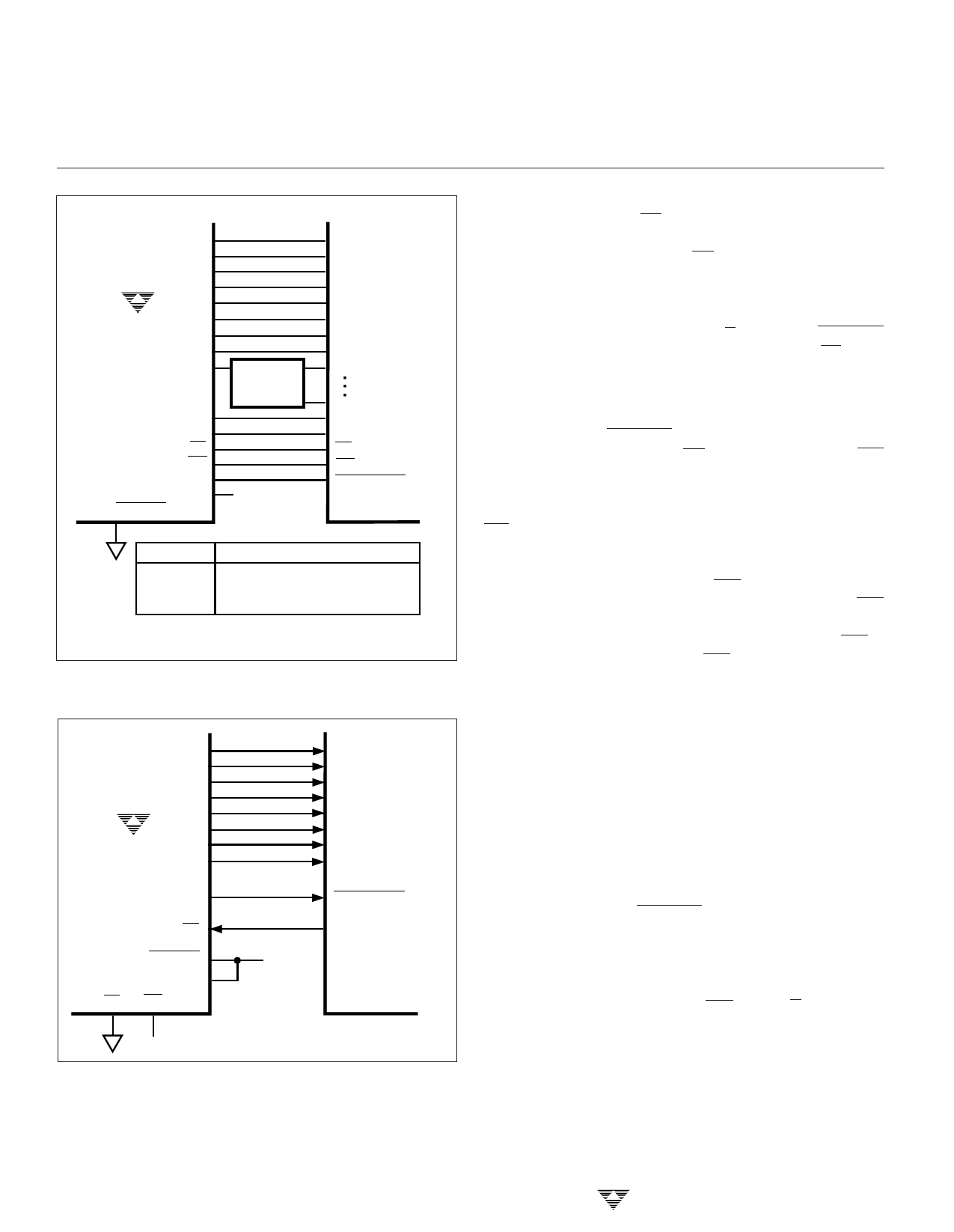
Figure 7. Interface to Typical µP Data Bus
TC850
DB0
DB1
DB2
DB3
DB4
DB5
DB6
DB7
BUSY
RD
CONT/DEMAND
CS
CS WR
PA0
PA1
PA2
PA3
PA4
PA5
PA6
PA7
µC OR µP
I/O PORT
INTERRUPT
PB0
+5V
NC
Figure 8. Interface to Typical µP I/O Port or Single-Chip µC
Since the PA0–PA7 inputs are dedicated to reading
A/D data, the A/D CS/CE inputs can be enabled continu-
ously. In continuous mode, data must be read in 3 bytes, as
shown in Table I. The required RD pulses are provided by a
µC/µP output pin.
The circuit of Figure 8 can also operate in the demand
mode, with the start-up conversion strobe generated by a
µC/µP output pin. In this case, the L/H and CONT/DEMAND
inputs can be controlled by I/O pins and the RD input
connected to digital ground.
Demand Mode Interface Timing
When CONT/DEMAND input is LOW, the TC850 per-
forms a conversion each time CE and CS are active and WR
is strobed LOW.
The demand mode conversion timing is shown in Figure
9. BUSY goes LOW and data is valid 1155 clock pulses after
WR goes LOW. After BUSY goes low, 125 additional clock
cycles are required before the next conversion cycle will
begin.
Once conversion is started, WR is ignored for 1100
internal clock cycles. After 1100 clock cycles, another WR
pulse is recognized and initiates a new conversion when the
present conversion is complete. A negative edge on WR is
required to begin conversion. If WR is held LOW, conver-
sions will not occur continuously.
The A/D conversion data is valid on the falling edge of
BUSY, and remains valid until one-half internal clock cycle
before BUSY goes HIGH on the succeeding conversion.
BUSY can be monitored with an I/O pin to determine end of
conversion, or to generate a µP interrupt.
In demand mode, the three data bytes can be read in
any desired order. The TC850 is simply regarded as three
bytes of memory and accessed accordingly. The bus output
timing is shown in Figure 10.
Continuous Mode Interface Timing
When the CONT/DEMAND input is HIGH, the TC850
performs conversions continuously. Data will be valid on the
falling edge of BUSY, and all three bytes must be read within
443-1/2 internal clock cycles of BUSY going LOW. The
timing diagram is shown in Figure 11.
In continuous mode, OVR/POL and L/H byte-select
inputs are ignored. The TC850 automatically cycles through
three data bytes, as shown in Table I. Bus output timing in
the continuous mode is shown in Figure 12.
3-88
TELCOM SEMICONDUCTOR, INC.
Share Link: