K9F2G08B0B データシートの表示(PDF) - Samsung
部品番号
コンポーネント説明
メーカー
K9F2G08B0B Datasheet PDF : 41 Pages
| |||
K9F2G08B0B
K9F2G08U0B
Preliminary
FLASH MEMORY
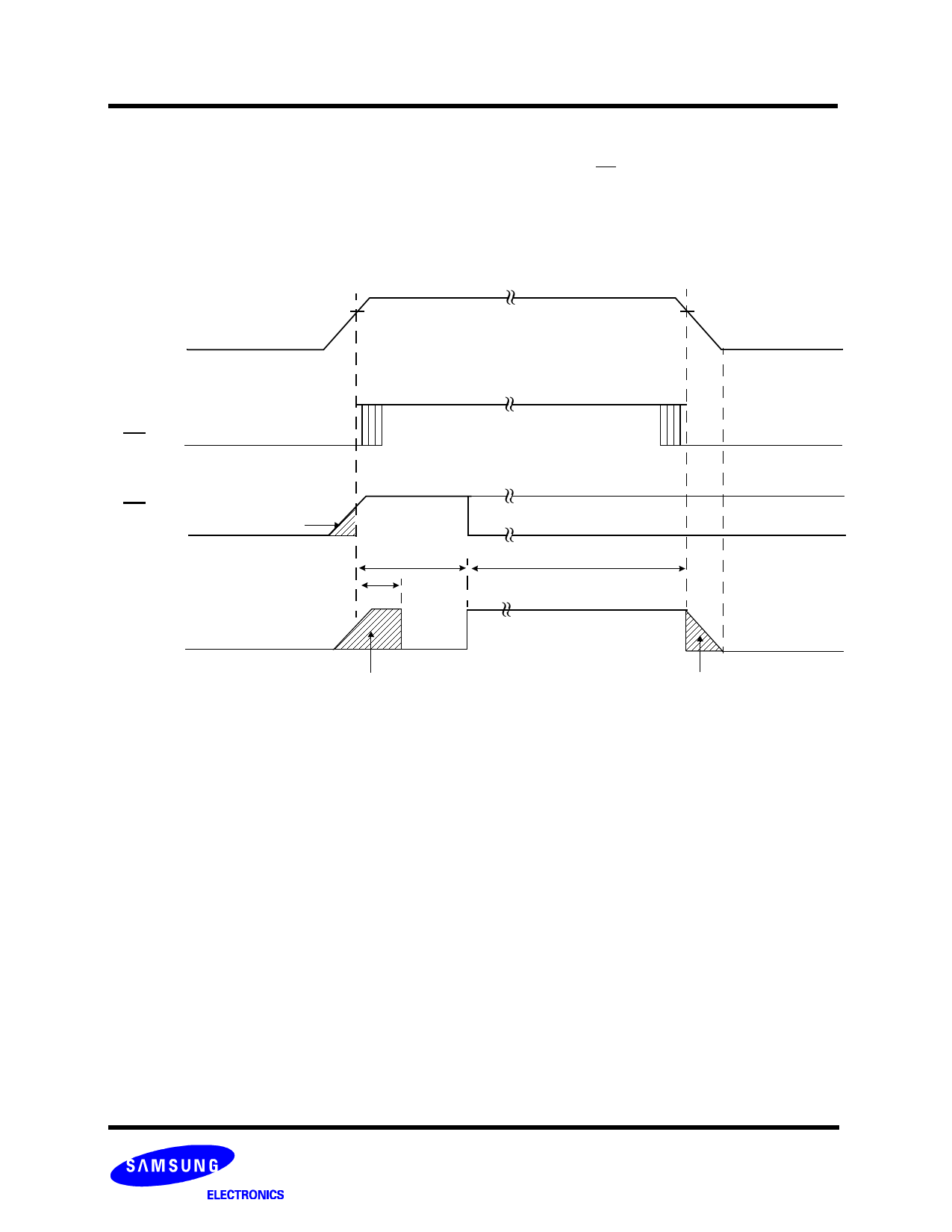
Data Protection & Power up sequence
The device is designed to offer protection from any involuntary program/erase during power-transitions. An internal voltage detector
disables all functions whenever Vcc is below about 1.8V(2.7V device), 2V(3.3V device). WP pin provides hardware protection and is
recommended to be kept at VIL during power-up and power-down. A recovery time of minimum 100µs is required before internal cir-
cuit gets ready for any command sequences as shown in Figure 20. The two step command sequence for program/erase provides
additional software protection.
Figure 20. AC Waveforms for Power Transition
~ 2.3V
VCC
High
~ 2.3V
WP
WE
Don’t care
Ready/Busy
5 ms max
100µs
Operation
Invalid
Note :During the initialization, the device consumes a maximum current of 30mA (ICC1)
Don’t care
Samsung Confidential
41
Share Link: 