AWT1921 データシートの表示(PDF) - ANADIGICS
部品番号
コンポーネント説明
メーカー
AWT1921 Datasheet PDF : 12 Pages
| |||
AWT1921
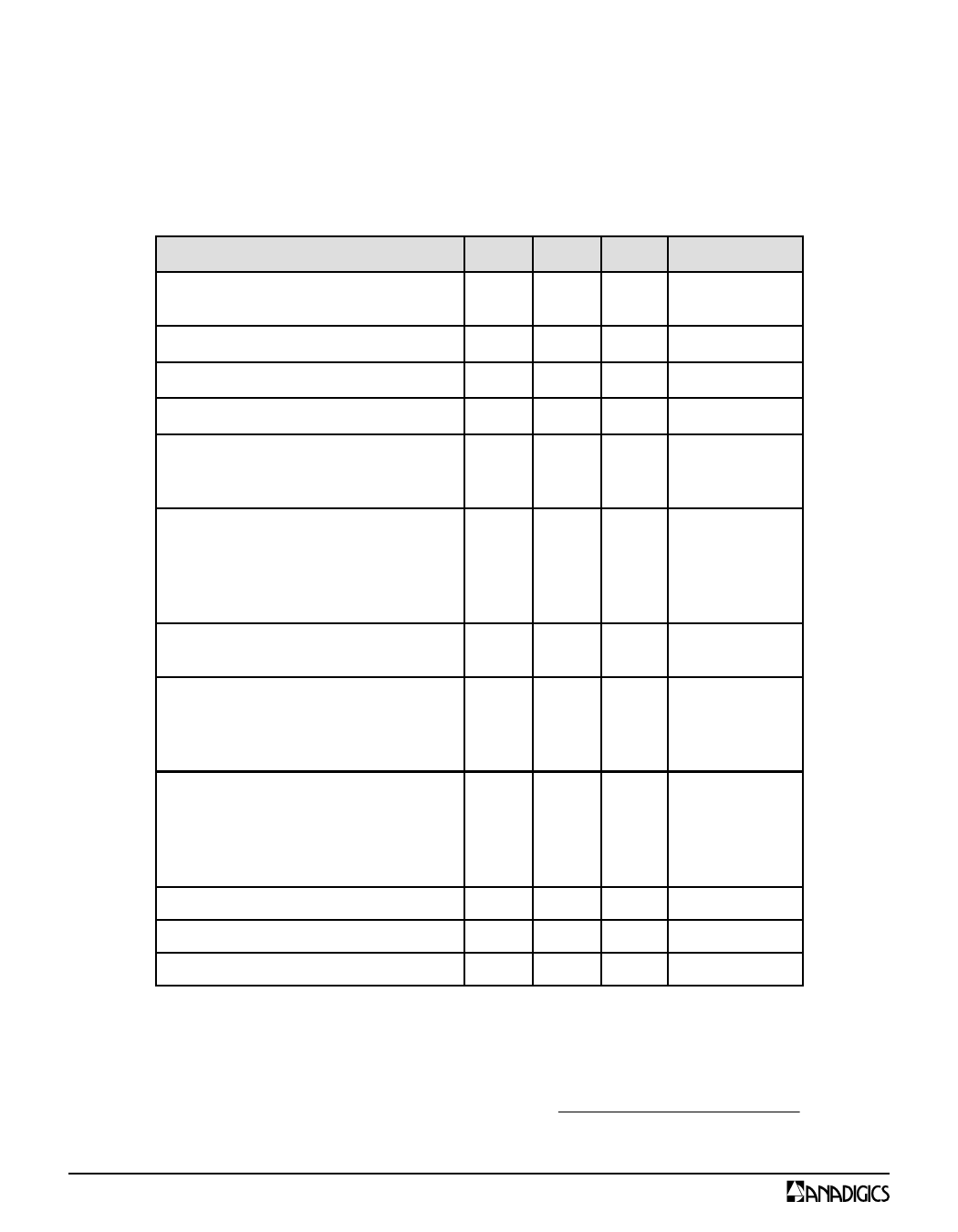
ELECTRICAL CHARACTERISTICS
Table 2: Electrical Specifications (1)
(Pin with CDMA modulation, fo = 1610 1626.5 MHz, VDS1 = VDS2 = VDS3
= VDS4 = 9.0V,VSS = -5V,VREF=+5V,VDD=+5V, Tc=25C, 50 W System(2))
PARAMETER
MIN TYP MAX
UNIT
Frequency
Power Output
Power Added Efficiency
Gain(3)
ACPR(3)
0.730 MHz
1.23 MHz
Harmonics
1610
35
-
27
-
-
1626.5
36
25
30
25
-28
100
2nd -
-45
3rd -
-52
4th -
-45
MHz
dBm
%
dB
dBc
dBc
Stability: - 60 dBc all spurious outputs
relative to desired signal
-
-
3:1
VSWR load, all
phase angles
Bias Supply Currents
ISS
IREF
IDD
Quiescent Currents
IDQ1
IDQ2
IDQ3
IDQ4
Input Return Loss
-
15
-
5
mA
-
15
-
-
-
-
60
90
150
200
-
-
-
-
mA
-
11
-
dB
Gain Flatness(3) @ POUT = +35 dBm
Thermal Resistance (4)
-
0.8
-
-
4.5
-
dB
C/W
Notes:
1. As measured in ANADIGICS test fixture, see application section.
2. 50W Measurement system after off chip matching circuit, input terminated in 50W.
3. Measured at POUT= +35 dBm
4. Thermal Resistance for junction to bottom of slug
Θjc
Tj −Tc
(ID1 + ID2 + ID3 + ID4)VSUP − POUT
2
PRELIMINARY DATA SHEET - Rev 1.0
08/2001
Share Link: 