Q67100-H3765 гғҮгғјгӮҝгӮ·гғјгғҲгҒ®иЎЁзӨәпјҲPDFпјү - Siemens AG
йғЁе“Ғз•ӘеҸ·
гӮігғігғқгғјгғҚгғігғҲиӘ¬жҳҺ
гғЎгғјгӮ«гғј
Q67100-H3765 Datasheet PDF : 26 Pages
| |||
SLx 24C64
7.1 Protection Bit Handling
The bits of the protection memory can be addressed directly for reading or programming.
A protection bit address corresponds to the lowest address within the respective page
(A5 to A12, A0 to A4 = zero). The status of each protection bit is sensed internally. A
written state (вҖң0вҖқ) prevents programming in the associated page. If an already protected
memory page is accidentally addressed for programming, the programming procedure
is suppressed.
The conventional I2C-Bus protocol allows data bytes to be read and programmed only.
Therefore an independent instruction sequence for addressing and manipulation of
protection bits is implemented. For protection bit instructions the command byte CSW
with its preceding START condition followed by the associated address bytes have to be
entered twice (figures 15 through 17). The first command byte CSW is followed by the
address bytes AHI/ALO with the bit/page address A0 through A4 always at zero. The
second CSW is required for entering a control byte CTx for protection bit manipulation.
The three control bytes for read, write or erase of a protection bit are listed below
(table 3):
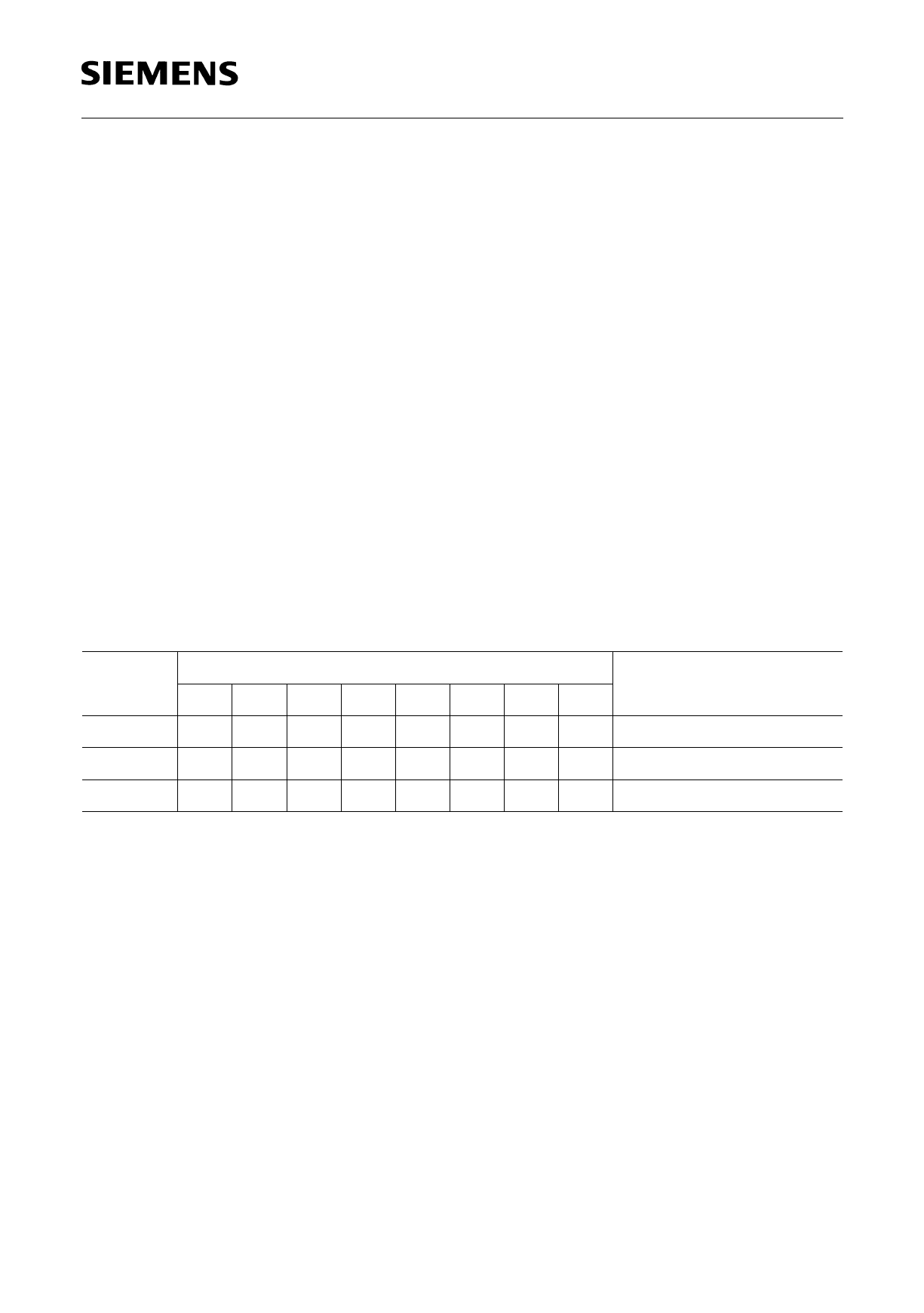
Table 3
Control Byte for Protection Bit Manipulation
Address
Definition
Function
Name
b7 b6 b5 b4 b3 b2 b1 b0
CTR
x x x x x x 0 0 Protection bit read
CTW
x x x x x x 0 1 Protection bit write
CTE
x x x x x x 1 1 Protection bit erase
Semiconductor Group
19
Preliminary 1998-07-27
Share Link: 