MAX1922ESA(2002) データシートの表示(PDF) - Maxim Integrated
部品番号
コンポーネント説明
メーカー
MAX1922ESA Datasheet PDF : 8 Pages
| |||
1A Current-Limited Switch for 2 USB Ports
cause a spurious OC output. Load-transient faults less
than 10ms (typ) will not cause an OC output assertion.
Only current-limit faults are blanked. Die overtempera-
ture faults and input voltage droops below the UVLO
threshold will cause an immediate OC output.
Applications Information
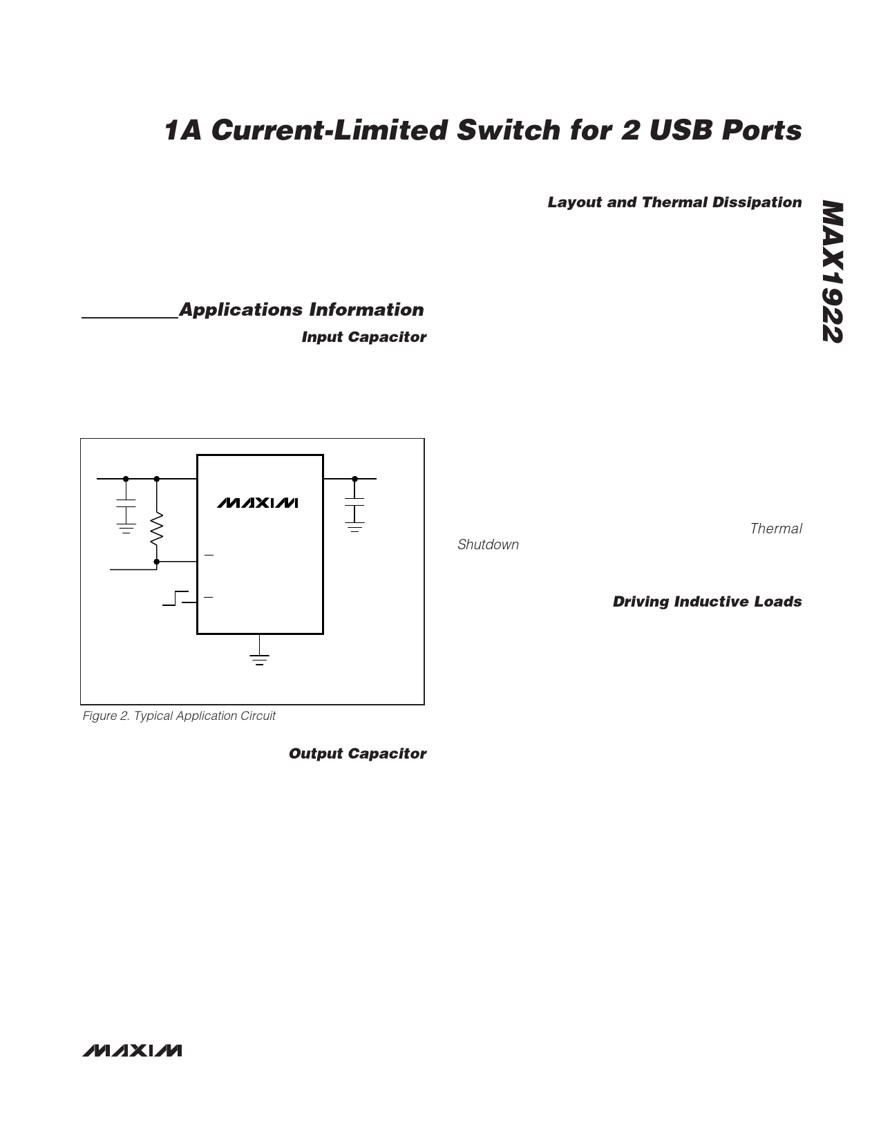
Input Capacitor
To limit the input voltage drop during momentary output
short-circuit conditions, connect a capacitor from IN to
GND. A 1µF ceramic capacitor will be adequate for
most applications; however, higher capacitor values will
further reduce the voltage drop at the input (Figure 2).
Output Capacitor
Connect a 0.1µF capacitor from OUT to GND. This
capacitor helps to prevent inductive parasitics from
pulling OUT negative during turn-off.
Layout and Thermal Dissipation
Important: Optimize the switch response time to output
short-circuit conditions by keeping all traces as short
as possible to reduce the effect of undesirable parasitic
inductance. Place input and output capacitors as close
as possible to the device (no more than 5mm away). All
IN and OUT pins must be connected with short traces
to the power bus. Wide power-bus planes will provide
superior heat dissipation through the MAX1922’s IN
and OUT pins.
INPUT
IN
OUT
1µF
OVERCURRENT
OUTPUT
100kΩ
MAX1922
OC
OFF
ON
EN
GND
OUTPUT
0.1µF*
Under normal operating conditions, the package can
dissipate and channel heat away. Calculate the maxi-
mum power dissipation as follows:
P = (ILIMIT)2 ✕ RON
where ILIMIT is the preset current limit (2.1A max) and
RON is the on-resistance of the switch (125mΩ max).
When the output is short circuited, foldback-current lim-
iting activates and the voltage drop across the switch
equals the input supply voltage. The power dissipated
across the switch increases, as does the die tempera-
ture. If the fault condition is not removed, the thermal-
overload protection circuitry activates (see Thermal
Shutdown section). Wide power-bus planes connected
to IN and OUT and a ground plane in contact with the
device help dissipate additional heat.
Driving Inductive Loads
A wide variety of devices (mice, keyboards, cameras,
and printers) can load the USB port. These devices
commonly connect to the port with cables, which can
add an inductive component to the load. This induc-
tance causes the output voltage at the USB port to ring
during a load step. The MAX1922 is capable of driving
inductive loads, but avoid exceeding the device’s
absolute maximum ratings. Usually the load inductance
is relatively small, and the MAX1922 input includes a
substantial bulk capacitance from an upstream regula-
tor as well as local bypass capacitors, limiting over-
shoot. If severe ringing occurs due to large load
inductance, clamp the MAX1922 output below 6V and
above -0.3V.
Chip Information
TRANSISTOR COUNT: 715
PROCESS: BiCMOS
*USB SPECIFICATIONS REQUIRE
A HIGHER VALUE CAPACITOR.
Figure 2. Typical Application Circuit
_______________________________________________________________________________________ 7
Share Link: 