MX25L4005MI-15 データシートの表示(PDF) - Macronix International
部品番号
コンポーネント説明
メーカー
MX25L4005MI-15 Datasheet PDF : 41 Pages
| |||
MX25L4005
(5) Write Status Register (WRSR)
The WRSR instruction is for changing the values of Status Register Bits. Before sending WRSR instruction, the Write
Enable (WREN) instruction must be decoded and executed to set the Write Enable Latch (WEL) bit in advance. The WRSR
instruction can change the value of Block Protect (BP2, BP1, BP0) bits to define the protected area of memory (as shown
in table 1). The WRSR also can set or reset the Status Register Write Disable (SRWD) bit in accordance with Write
Protection (WP#) pin signal. The WRSR instruction cannot be executed once the Hardware Protected Mode (HPM) is
entered.
The sequence of issuing WRSR instruction is: CS# goes low-> sending WRSR instruction code-> Status Register data
on SI-> CS# goes high. (see Figure 15)
The WRSR instruction has no effect on b6, b5, b1, b0 of the status register.
The CS# must go high exactly at the byte boundary; otherwise, the instruction will be rejected and not executed. The self-
timed Write Status Register cycle time (tW) is initiated as soon as Chip Select (CS#) goes high. The Write in Progress
(WIP) bit still can be check out during the Write Status Register cycle is in progress. The WIP sets 1 during the tW timing,
and sets 0 when Write Status Register Cycle is completed, and the Write Enable Latch (WEL) bit is reset.
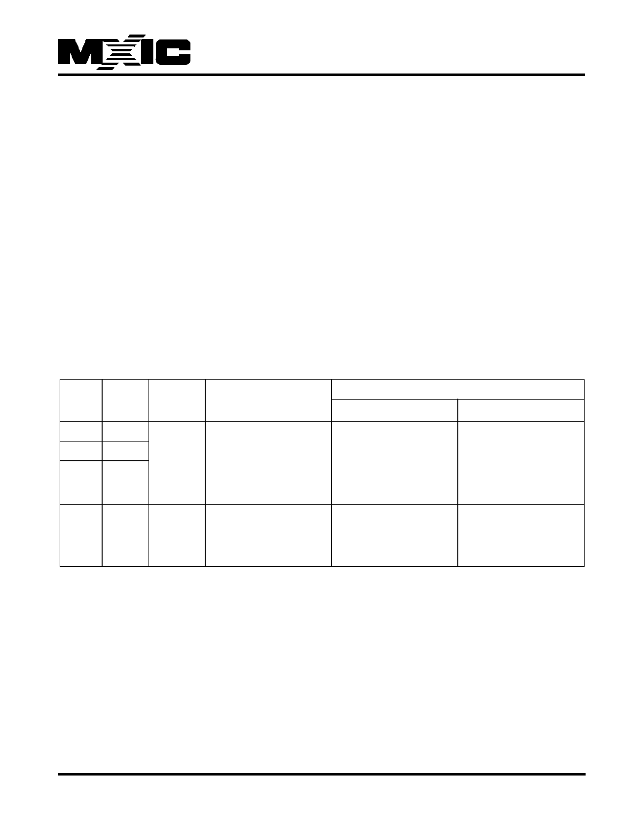
Table 4. Protection Modes
WP# SRWD
Signal Bit
Mode
Write Protection of the
Status Register
Memory Content
Protected Area1
Unprotected Area1
1
0
Status Register is
Writable (if the WREN
0
0
Software instruction has set the
Protected against Page
Ready to accept Page
Protected WEL bit)
Program, Sector Erase
Program and Sector
(SPM) The values in the SRWD, and Chip Erase
Erase instructions
1
1
BP2, BP1 and BP0
bits can be changed
Status Register is
Hardware Hardware write protected Protected against Page
Ready to accept Page
0
1
Protected The values in the SRWD, Program, Sector Erase
Program and Sector
(HPM) BP2, BP1 and BP0
and Chip Erase
Erase instructions
bits cannot be changed
Note:
1. As defined by the values in the Block Protect (BP2, BP1, BP0) bits of the Status Register, as shown in Table 1.
As the above table showing, the summary of the Software Protected Mode (SPM) and Hardware Protected Mode (HPM).
Software Protected Mode (SPM):
- When SRWD bit=0, no matter WP# is low or high, the WREN instruction may set the WEL bit and can change the values
of SRWD, BP2, BP1, BP0. The protected area, which is defined by BP2, BP1, BP0, is at software protected mode
(SPM).
- When SRWD bit=1 and WP# is high, the WREN instruction may set the WEL bit can change the values of SRWD, BP2,
BP1, BP0. The protected area, which is defined by BP2, BP1, BP0, is at software protected mode (SPM)
P/N: PM1236
REV. 1.1, SEP. 30, 2005
12
Share Link: 