UPD784038YGC-XXX-8BT データシートの表示(PDF) - NEC => Renesas Technology
部品番号
コンポーネント説明
メーカー
UPD784038YGC-XXX-8BT Datasheet PDF : 94 Pages
| |||
µPD784035Y, 784036Y, 784037Y, 784038Y
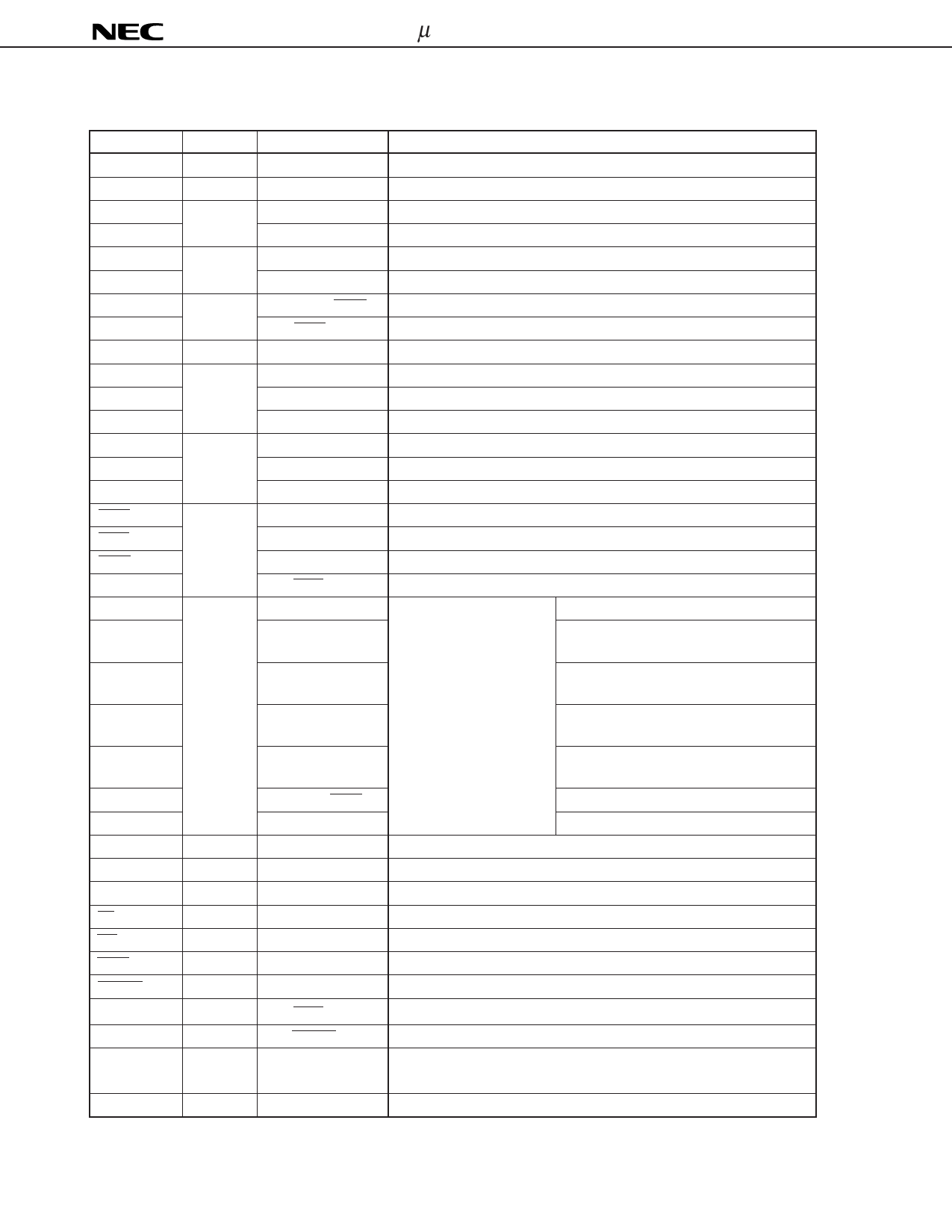
5.2 Non-Port Pins
Pin Name
TO0 to TO3
CI
RxD
RxD2
TxD
TxD2
ASCK
ASCK2
SDA
SI0
SI1
SI2
SO0
SO1
SO2
SCK0
SCK1
SCK2
SCL
NMI
INTP0
INTP1
INTP2
INTP3
INTP4
INTP5
AD0 to AD7
A8 to A15
A16 to A19
RD
WR
WAIT
REFRQ
HLDRQ
HLDAK
ASTB
CLKOUT
I/O
Output
Input
Input
Output
Input
I/O
Input
Output
I/O
Input
I/O
Output
Output
Output
Output
Input
Output
Input
Output
Output
Output
Alternate function
P34 to P37
P23/INTP2
P30/SI1
P13/SI2
P31/SO1
P14/SO2
P25/INTP4/SCK1
P12/SCK2
P33/SO0
P27
P30/RxD
P13/RxD2
P33/SDA
P31/TxD
P14/TxD2
P32/SCL
P25/INTP4/ASCK
P12/ASCK2
P32/SCK0
P20
P21
P22
P23/CI
P24
P25/ASCK/SCK1
P26
P40 to P47
P50 to P57
P60 to P63
P64
P65
P66/HLDRQ
P67/HLDAK
P66/WAIT
P67/REFRQ
CLKOUT
ASTB
Function
Timer output
Count clock input to timer/counter 2
Serial data input (UART0)
Serial data input (UART2)
Serial data output (UART0)
Serial data output (UART2)
Baud rate clock input (UART0)
Baud rate clock input (UART2)
Serial data input/output (2-wire serial I/O, I2C bus)
Serial data input (3-wire serial I/O0)
Serial data input (3-wire serial I/O1)
Serial data input (3-wire serial I/O2)
Serial data output (3-wire serial I/O0)
Serial data output (3-wire serial I/O1)
Serial data output (3-wire serial I/O2)
Serial clock input/output (3-wire serial I/O0)
Serial clock input/output (3-wire serial I/O1)
Serial clock input/output (3-wire serial I/O2)
Serial clock input/output (2-wire serial I/O, I2C bus)
External interrupt requests
–
• Count clock input to timer/counter 1
• Capture trigger signal of CR11 or CR12
• Count clock input to timer/counter 2
• Capture trigger signal of CR22
• Count clock input to timer/counter 2
• Capture trigger signal of CR21
• Count clock input to timer/counter 0
• Capture trigger signal of CR02
–
Conversion start trigger input to A/D converter
Time-division address/data bus (for external memory connection)
Higher address bus (for external memory connection)
Higher address when address is extended (for external memory connection)
Read strobe to external memory
Write strobe to external memory
Wait insertion
Refresh pulse output to external pseudo static memory
Bus hold request input
Bus hold acknowledge output
Latch timing output of time-division address (A0 through A7)
(when accessing external memory)
Clock output
14
Share Link: 