MAX8969EWL53 データシートの表示(PDF) - Maxim Integrated
部品番号
コンポーネント説明
メーカー
MAX8969EWL53 Datasheet PDF : 18 Pages
| |||
MAX8969
Step-Up Converter for Handheld Applications
Absolute Maximum Ratings
IN, OUT_ to GND_................................................-0.3V to +6.0V
EN, TREN to GND_............ -0.3V to lower of (VIN + 0.3V) or 6V
Total LX_ RMS Current (Note 1)....................................3.2ARMS
OUT_ Short Circuit to GND_......................................Continuous
Continuous Power Dissipation (TA = +70°C)
WLP (derate 12mW/NC above +70°C)........................960mW
Operating Temperature Range.............................-40ºC to +85°C
Junction Temperature.......................................................+150°C
Storage Temperature Range............................. -65°C to +150°C
Soldering Temperature (reflow) (Note 2).......................... +260°C
Note 1: LX_ has internal silicon diodes to GND_ and OUT_. It is normal for these diodes to briefly conduct during LX_ transitions.
Avoid steady state conduction of these diodes.
Note 2: This device is constructed using a unique set of packaging techniques that impose a limit on the thermal profile that the
device can be exposed to during board level solder attach and rework. This limit permits only the use of the solder pro-
files recommended in the industry-standard specification JEDEC 020A, paragraph 7.6, Table 3 for IR/VPR and Convection
reflow. Preheating is required. Hand or wave soldering is not allowed.
Stresses beyond those listed under “Absolute Maximum Ratings” may cause permanent damage to the device. These are stress ratings only, and functional operation
of the device at these or any other conditions beyond those indicated in the operational sections of the specifications is not implied. Exposure to absolute maximum
rating conditions for extended periods may affect device reliability.
Package Thermal Characteristics (Note 1)
WLP
Junction-to-Ambient Thermal Resistance (θJA)...........83°C/W
Junction-to-Case Thermal Resistance (θJC)................50°C/W
Note 3: Package thermal resistances were obtained using the method described in JEDEC specification JESD51-7, using a four-layer
board. For detailed information on package thermal considerations, refer to www.maximintegrated.com/thermal-tutorial.
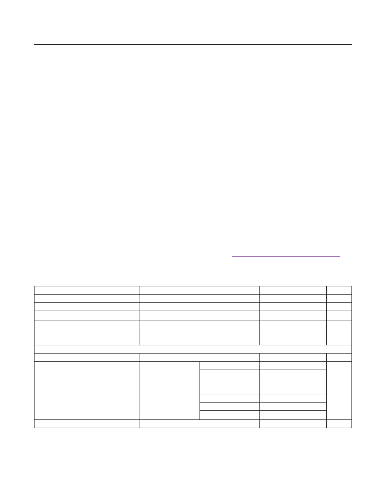
Electrical Characteristics
(VIN = 2.6V, TA = -40°C to +85°C, unless otherwise noted. Typical values are TA = +25°C.) (Note 4)
PARAMETER
Operating Input Voltage Range
CONDITIONS
MIN
2.5
Minimum Startup Voltage
Undervoltage Lockout Threshold (UVLO) VIN falling, 75mV hysteresis
2.1
Shutdown Supply Current
VEN = VTREN = VOUT = 0V,
VIN = 4.8V
TA = +25°C
TA = +85°C
Thermal Shutdown Temperature
TJ rising, 20°C hysteresis
BOOST MODE
Peak Output Current
VIN > 2.5V, pulse loading (Note 5)
VOUT = 3.3V
VOUT = 3.5V
Minimum Continuous Output Current
VIN > 2.5V (Note 5)
VOUT = 3.7V
VOUT = 4.25V
VOUT = 5.0V
VOUT = 5.3V
VOUT = 5.5V
Switching Frequency
(Note 6)
TYP
2.3
2.2
0.8
1
+165
MAX
5.5
2.3
5
UNITS
V
V
V
µA
°C
1
A
0.9
0.8
0.7
0.7
A
0.7
0.7
0.7
3
MHz
www.maximintegrated.com
Maxim Integrated │ 2
Share Link: 