F64P30B8E2T085 データシートの表示(PDF) - Intel
部品番号
コンポーネント説明
メーカー
F64P30B8E2T085 Datasheet PDF : 102 Pages
| |||
1-Gbit P30 Family
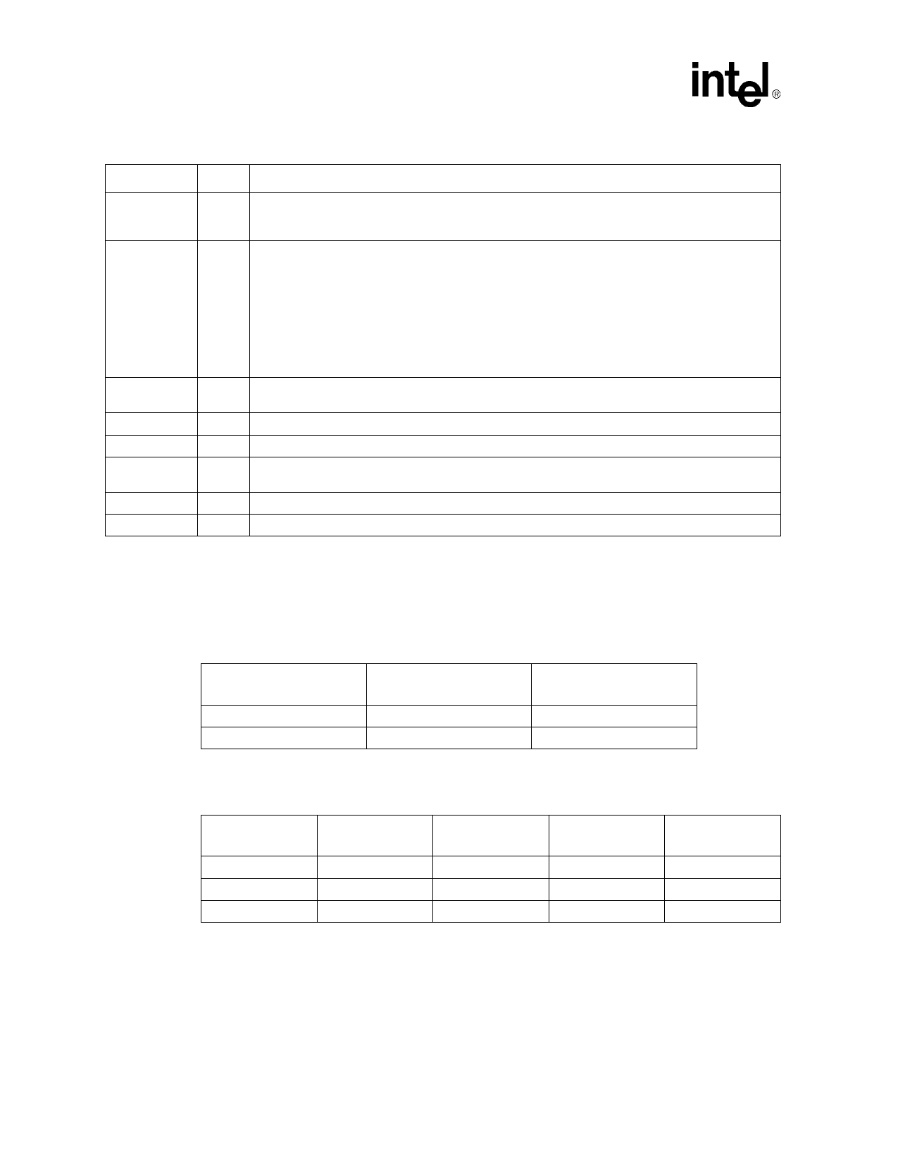
Table 4.
Symbol
WP#
VPP
VCC
VCCQ
VSS
RFU
DU
NC
QUAD+ SCSP Signal Descriptions (Sheet 2 of 2)
Type
Name and Function
Input
WRITE PROTECT: Active low input. WP# low enables the lock-down mechanism. Blocks in lock-
down cannot be unlocked with the Unlock command. WP# high overrides the lock-down function
enabling blocks to be erased or programmed using software commands.
Power/
lnput
Erase and Program Power: A valid voltage on this pin allows erasing or programming. Memory
contents cannot be altered when VPP ≤ VPPLK. Block erase and program at invalid VPP voltages
should not be attempted.
Set VPP = VCC for in-system program and erase operations. To accommodate resistor or diode drops
from the system supply, the VIH level of VPP can be as low as VPPL min. VPP must remain above VPPL
min to perform in-system flash modification. VPP may be 0 V during read operations.
VPPH can be applied to main blocks for 1000 cycles maximum and to parameter blocks for 2500
cycles. VPP can be connected to 9 V for a cumulative total not to exceed 80 hours. Extended use of
this pin at 9 V may reduce block cycling capability.
Power
Power
Device Core Power Supply: Core (logic) source voltage. Writes to the flash array are inhibited when
VCC ≤ VLKO. Operations at invalid VCC voltages should not be attempted.
Output Power Supply: Output-driver source voltage.
Power Ground: Connect to system ground. Do not float any VSS connection.
—
Reserved for Future Use: Reserved by Intel for future device functionality and enhancement. These
should be treated in the same way as a Do Not Use (DU) signal.
— Do Not Use: Do not connect to any other signal, or power supply; must be left floating.
— No Connect: No internal connection; can be driven or floated.
4.3
SCSP Configurations
Table 5.
Stacked Easy BGA Chip Select Logic
Stack Combination
1-die
2-die
Selected Flash
Die #1
F1-CE#
F1-CE# + A25 (VIL)
Selected Flash
Die #2
-
F1-CE# + A25 (VIH)
Table 6.
QUAD+ SCSP Chip Select Logic
Stack
Combination
1-die
2-die
4-die
Selected Flash
Die #1
Selected Flash
Die #2
Selected Flash
Die #3
Selected Flash
Die #4
F1-CE#
-
-
-
F1-CE# + A24 (VIL) F1-CE# + A24 (VIH)
-
-
F1-CE# + A24 (VIL) F1-CE# + A24 (VIH) F2-CE# + A24 (VIL) F2-CE# + A24 (VIH)
April 2005
22
Intel StrataFlash® Embedded Memory (P30)
Order Number: 306666, Revision: 001
Datasheet
Share Link: 