28F256L18 データシートの表示(PDF) - Numonyx -> Micron
部品番号
コンポーネント説明
メーカー
28F256L18 Datasheet PDF : 106 Pages
| |||
Numonyx™ StrataFlash® Wireless Memory (L18)
4.2
Signal Descriptions
This section includes signal descriptions for the following packages:
• VF BGA Package Signal Descriptions
• SCSP Package Signal Descriptions
4.2.1
VF BGA Package Signal Descriptions
Table 1 describes the active signals used on the Numonyx™ StrataFlash® Wireless
Memory (L18), VF BGA package.
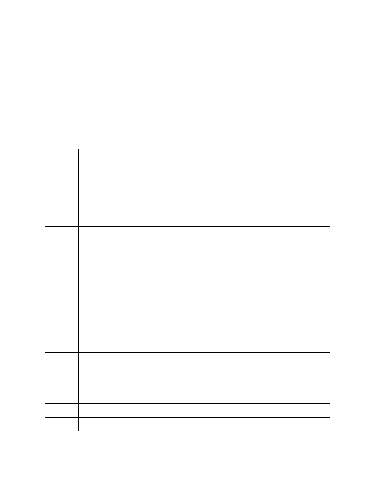
Table 1: Signal Descriptions (Sheet 1 of 2)
Symbol
A[MAX:0]
DQ[15:0]
ADV#
CE#
CLK
OE#
RST#
WAIT
WE#
WP#
VPP
VCC
VCCQ
Type
Name and Function
Input ADDRESS: Device address inputs. 128-Mbit: A[22:0]; 256-Mbit: A[23:0].
DATA INPUT/OUTPUTS: Inputs data and commands during write cycles; outputs data during
Input/ memory, Status Register, Protection Register, and Read Configuration Register reads. Data balls float
Output
when the CE# or OE# are deasserted. Data is internally latched during writes.
Input
ADDRESS VALID: Active-low input. During synchronous read operations, addresses are latched on
the rising edge of ADV#, or on the next valid CLK edge with ADV# low, whichever occurs first.
In asynchronous mode, the address is latched when ADV# going high or continuously flows through if
ADV# is held low.
CHIP ENABLE: Active-low input. CE#-low selects the device. CE#-high deselects the device, placing it
Input in standby, with DQ[15:0] and WAIT in High-Z.
Input
CLOCK: Synchronizes the device with the system’s bus frequency in synchronous-read mode and
increments the internal address generator. During synchronous read operations, addresses are latched
on the rising edge of ADV#, or on the next valid CLK edge with ADV# low, whichever occurs first.
OUTPUT ENABLE: Active-low input. OE#-low enables the device’s output data buffers during read
Input cycles. OE#-high places the data outputs in High-Z and WAIT in High-Z.
Input
RESET: Active-low input. RST# resets internal automation and inhibits write operations. This provides
data protection during power transitions. RST#-high enables normal operation. Exit from reset places
the device in asynchronous read array mode.
Output
WAIT: Indicates data valid in synchronous array or non-array burst reads. Configuration Register bit
10 (RCR[10], WT) determines its polarity when asserted. With CE# and OE# at VIL, WAIT’s active
output is VOL or VOH when CE# and OE# are asserted. WAIT is high-Z if CE# or OE# is VIH.
• In synchronous array or non-array read modes, WAIT indicates invalid data when asserted and
valid data when deasserted.
• During asynchronous reads, WAIT is deasserted.
• During writes (when OE# is deasserted), WAIT is tristated.
WRITE ENABLE: Active-low input. WE# controls writes to the device. Address and data are latched on
Input
the rising edge of WE#.
Input
WRITE PROTECT: Active-low input. WP#-low enables the lock-down mechanism. Blocks in lock-down
cannot be unlocked with the Unlock command. WP#-high overrides the lock-down function enabling
blocks to be erased or programmed using software commands.
Power/
lnput
Erase and Program Power: A valid voltage on this pin allows erasing or programming. Memory
contents cannot be altered when VPP ≤ VPPLK. Block erase and program at invalid VPP voltages should
not be attempted.
Set VPP = VCC for in-system program and erase operations. To accommodate resistor or diode drops
from the system supply, the VIH level of VPP can be as low as VPPLmin. VPP must remain above VPPLmin
to perform in-system program or erase. VPP may be 0 V during read operations.
VPPH can be applied to main blocks for 1000 cycles maximum and to parameter blocks for 2500 cycles.
VPP can be connected toVPPH for a cumulative total not to exceed 80 hours. Extended use of this pin at
VPPH may derate flash performance/behavior.
Device Core Power Supply: Core (logic) source voltage. Writes to the flash array are inhibited when
Power VCC ≤ VLKO. Operations at invalid VCC voltages should not be attempted.
Power Output Power Supply: Output-driver source voltage. This ball can be tied directly to VCC if operating
within VCC range.
Datasheet
18
November 2007
251902-12
Share Link: 