28F128L18 データシートの表示(PDF) - Numonyx -> Micron
部品番号
コンポーネント説明
メーカー
28F128L18 Datasheet PDF : 106 Pages
| |||
Numonyx™ StrataFlash® Wireless Memory (L18)
Table 1: Signal Descriptions (Sheet 2 of 2)
Symbol
Type
Name and Function
VSS
VSSQ
DU
RFU
Power Ground: Ground reference for device logic voltages. Connect to system ground.
Power Ground: Ground reference for device output voltages. Connect to system ground.
—
Do Not Use: Do not use this ball. This ball should not be connected to any power supplies, signals or
other balls, and must be left floating.
— Reserved for Future Use: Reserved by Numonyx for future device functionality and enhancement.
4.2.2
128/0 and 256/0 SCSP Package Signal Descriptions
Table 2 describes the active signals used on the 128/0 and 256/0 SCSP.
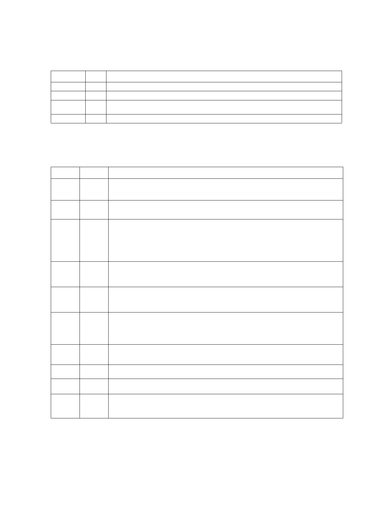
Table 2:
Symbol
A[Max:0]
DQ[15:0]
F1-CE#
F2-CE#
F3-CE#
S-CS1#
S-CS2
P-CS#
F1-OE#
F2-OE#
R-OE#
WE#
R-WE#
CLK
Device Signal Descriptions for SCSP (Sheet 1 of 2)
Type
Input
Input/
Output
Input
Input
Input
Input
Input
Input
Input
Input
Description
ADDRESS INPUTS: Inputs for all die addresses during read and write operations.
• 128-Mbit Die: A[Max] = A22
• 256-Mbit Die: A[Max] = A23
DATA INPUTS/OUTPUTS: Inputs data and commands during write cycles, outputs data during read
cycles. Data signals float when the device or its outputs are deselected. Data is internally latched
during writes.
FLASH CHIP ENABLE: Low-true: selects the associated flash memory die. When asserted, flash
internal control logic, input buffers, decoders, and sense amplifiers are active. When deasserted, the
associated flash die is deselected, power is reduced to standby levels, data and WAIT outputs are
placed in high-Z state.
F1-CE# selects the flash die.
F2-CE# and F3-CE# are available on stacked combinations with two or three flash dies else they are
RFU. They each can be tied high to VCCQ through a 10K-ohm resistor for future design flexibility.
SRAM CHIP SELECTS: When both SRAM chip selects are asserted, SRAM internal control logic, input
buffers, decoders, and sense amplifiers are active. When either/both SRAM chip selects are deasserted
(S-CS1# = VIH or S-CS2 = VIL), the SRAM is deselected and its power is reduced to standby levels.
Treat this signal as NC (No Connect) for this device.
PSRAM CHIP SELECT: Low-true; when asserted, PSRAM internal control logic, input buffers,
decoders, and sense amplifiers are active. When deasserted, the PSRAM is deselected and its power is
reduced to standby levels.
Treat this signal as NC (No Connect) for this device.
FLASH OUTPUT ENABLE: Low-true; enables the flash output buffers. OE#-high disables the flash
output buffers, and places the flash outputs in High-Z.
F1-OE# controls the outputs of the flash die.
F2-OE# is available on stacked combinations with two or three flash dies else it is RFU. It can be pulled
high to VCCQ through a 10K-ohm resistor for future design flexibility.
RAM OUTPUT ENABLE: Low-true; R-OE#-low enables the selected RAM output buffers. R-OE#-high
disables the RAM output buffers, and places the selected RAM outputs in High-Z.
Treat this signal as NC (No Connect) for this device.
FLASH WRITE ENABLE: Low-true; WE# controls writes to the selected flash die. Address and data
are latched on the rising edge of WE#.
RAM WRITE ENABLE: Low-true; R-WE# controls writes to the selected RAM die.
Treat this signal as NC (No Connect) for this device.
FLASH CLOCK: Synchronizes the device with the system’s bus frequency in synchronous-read mode
and increments the internal address generator. During synchronous read operations, addresses are
latched on the rising edge of ADV#, or on the next valid CLK edge with ADV# low, whichever occurs
first.
November 2007
251902-12
Datasheet
19
Share Link: 