AD5533BBCZ-1 データシートの表示(PDF) - Analog Devices
部品番号
コンポーネント説明
メーカー
AD5533BBCZ-1 Datasheet PDF : 16 Pages
| |||
AD5533B
MSB
LSB
0
0
CAL
OFFSET SEL
0
A4–A0
MODE BIT 1 MODE BIT 2
MODE BITS
TEST BIT
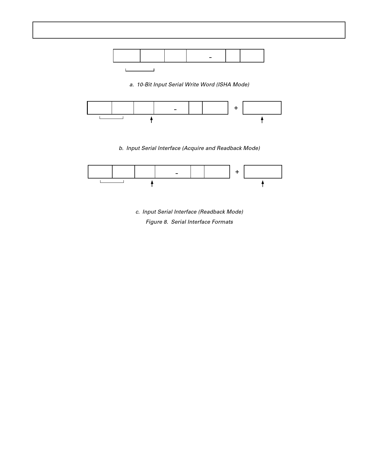
a. 10-Bit Input Serial Write Word (ISHA Mode)
MSB
LSB
MSB
LSB
1
0
CAL
OFFSET SEL
0
A4–A0
DB1 3 –DB0
MODE BITS
10-BIT
SERIAL WORD
WRITTEN TO PART
TEST BIT
14-BIT DATA
READ FROM PART AFTER
NEXT FALLING EDGE OF SYNC
(DB13 = MSB OF DAC WORD)
b. Input Serial Interface (Acquire and Readback Mode)
MSB
1
1
MODE BITS
LSB
MSB
LSB
0
OFFSET SEL
0
A4–A0
DB1 3 –DB0
10-BIT
SERIAL WORD
WRITTEN TO PART
TEST BIT
14-BIT DATA
READ FROM PART AFTER
NEXT FALLING EDGE OF SYNC
(DB13 = MSB OF DAC WORD)
c. Input Serial Interface (Readback Mode)
Figure 8. Serial Interface Formats
DB13–DB0 Bit
These are used in both readback modes to read a 14-bit word
from the addressed DAC register.
The serial interface is designed to allow easy interfacing to most
microcontrollers and DSPs, e.g., PIC16C, PIC17C, QSPI™,
SPI™, DSP56000, TMS320, and ADSP-21xx, without the
need for any glue logic. When interfacing to the 8051, the
SCLK must be inverted. The Microprocessor/Microcontroller
Interface section explains how to interface to some popular
DSPs and microcontrollers.
Figures 3 and 4 show the timing diagram for a serial read and
write to the AD5533B. The serial interface works with both a
continuous and a noncontinuous serial clock. The first falling
edge of SYNC resets a counter that counts the number of serial
clocks to ensure the correct number of bits are shifted in and out
of the serial shift registers. Any further edges on SYNC are ignored
until the correct number of bits are shifted in or out. Once the
correct number of bits have been shifted in or out, the SCLK is
ignored. In order for another serial transfer to take place, the
counter must be reset by the falling edge of SYNC. In readback,
the first rising SCLK edge after the falling edge of SYNC causes
DOUT to leave its high impedance state and data is clocked out
onto the DOUT line and also on subsequent SCLK rising edges.
The DOUT pin goes back into a high impedance state on the falling
edge of the 14th SCLK. Data on the DIN line is latched in on the
first SCLK falling edge after the falling edge of the SYNC signal
and on subsequent SCLK falling edges. The serial interface will
not shift data in or out until it receives the falling edge of the
SYNC signal.
*SPI and QSPI are trademarks of Motorola, Inc.
Parallel Interface
The SER/PAR bit is tied low to enable the parallel interface and
disable the serial interface. The parallel interface is controlled
by nine pins as follows:
CS
Active low package select pin. This pin is shared with the
SYNC function for the serial interface.
WR
Active low write pin. The values on the address pins are
latched on a rising edge of WR.
A4–A0
Five address pins (A4 = MSB of address, A0 = LSB). These
are used to address the relevant channel (out of a possible 32).
Offset_Sel
Offset select pin. This has the same function as the Offset_Sel
bit in the serial interface. When it is high, the offset channel
is addressed and the address on A4–A0 is ignored.
Cal
Same functionality as the Cal bit in the serial interface. When
this pin is high, all 32 channels acquire VIN simultaneously.
MICROPROCESSOR INTERFACING
AD5533B to ADSP-21xx Interface
The ADSP-21xx family of DSPs is easily interfaced to the
AD5533B without the need for extra logic.
A data transfer is initiated by writing a word to the TX register
after the SPORT has been enabled. In a write sequence, data is
clocked out on each rising edge of the DSP’s serial clock and
clocked into the AD5533B on the falling edge of its SCLK. In
REV. A
–13–
Share Link: 