AD818(2000) データシートの表示(PDF) - Analog Devices
部品番号
コンポーネント説明
メーカー
AD818 Datasheet PDF : 12 Pages
| |||
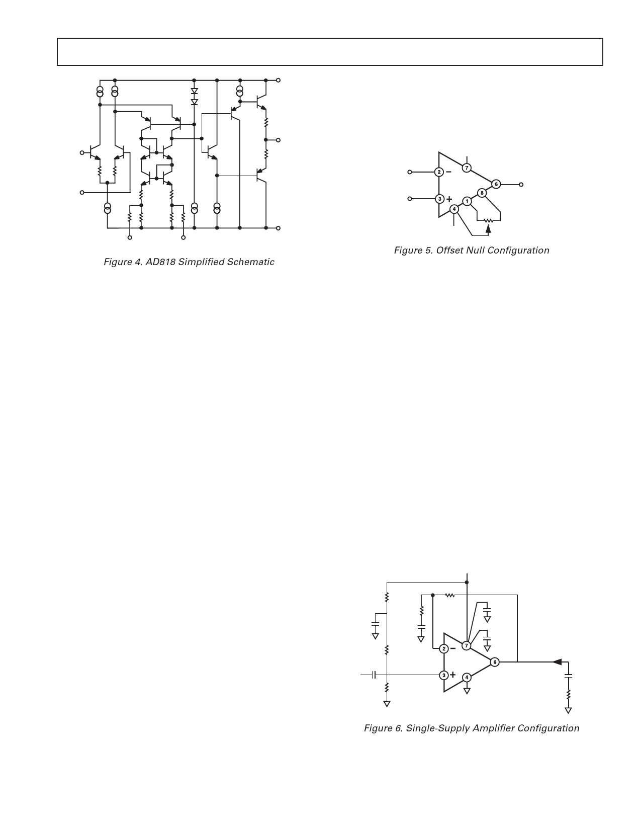
AD818
ERROR
SIGNAL
OUTPUT
ERROR AMPLIFIER
VERROR OUTPUT × 10
2×
HP2835
3
5
AD829
2×
HP2835
100Ω
6
2
4
7
0.47µF
1MΩ
15pF
SHORT, DIRECT
CONNECTION TO
TEKTRONIX TYPE 11402
OSCILLOSCOPE PREAMP
INPUT SECTION
0 TO ±10V
POWER
SUPPLY
EI&S
DL1A05GM
MERCURY
RELAY
7, 8
2
FALSE
NULL SUMMING
ADJUST NODE
1kΩ 100Ω 500Ω 1kΩ
TTL LEVEL
SIGNAL
GENERATOR
50Hz
OUTPUT
13
1, 14
DIGITAL
GROUND
ANALOG
GROUND
50Ω
COAX
CABLE
500Ω
50 Ω
5–18pF
2
AD818 6
3
4
7
2.2µF
2.2µF
0.01µF
–VS
+VS
0.01µF
0.47µF
–VS
1.9k Ω +VS
0.01µF
100Ω
DEVICE
UNDER
TEST
0.01µF
NOTE:
USE CIRCUIT BOARD
WITH GROUND PLANE
10pF
SCOPE PROBE
CAPACITANCE
TEKTRONIX P6201
FET PROBE TO
TEKTRONIX TYPE 11402
OSCILLOSCOPE
PREAMP INPUT SECTION
SETTLING
OUTPUT
Figure 37. Settling Time Test Circuit
AD818 SETTLING TIME
Settling time is comprised primarily of two regions. The first is
the slew time in which the amplifier is overdriven, where the
output voltage rate of change is at its maximum. The second is
the linear time period required for the amplifier to settle to
within a specified percent of the final value.
Measuring the rapid settling time of AD818 (45 ns to 0.1% and
80 ns to 0.01%—10 V step) requires applying an input pulse
with a very fast edge and an extremely flat top. With the AD818
configured in a gain of –1, a clamped false summing junction
responds when the output error is within the sum of two diode
voltages (approximately 1 volt). The signal is then amplified 20
times by a clamped amplifier whose output is connected directly
to a sampling oscilloscope.
A High Performance Video Line Driver
The buffer circuit shown in Figure 38 will drive a back-termi-
nated 75 Ω video line to standard video levels (1 V p-p) with
0.1 dB gain flatness to 55 MHz with only 0.05° and 0.01%
differential phase and gain at the 3.58 MHz NTSC subcarrier
frequency. This level of performance, which meets the require-
ments for high-definition video displays and test equipment, is
achieved using only 7 mA quiescent current.
DIFFERENTIAL LINE RECEIVER
The differential receiver circuit of Figure 39 is useful for many
applications from audio to video. It allows extraction of a low
level signal in the presence of common-mode noise. As shown
in Figure 40, the AD818 provides this function with only
10 nV/√Hz noise at the output.
2pF
1k⍀
1k⍀
DIFFERENTIAL
INPUT
1k⍀
+5V
0.01F
2.2F
2
7
AD818
3
4
6
VOUT
0.01F
2.2F
–5V
1k⍀
2pF
OUTPUT
Figure 39. Differential Line Receiver
+15V
0.01µF
2.2µF
VIN
Rt
75Ω
2
7
AD818 6
3
4
0.01µF
Rbt
75 Ω
75Ω
Rt
75Ω
2.2µF
1k Ω
–15V
1k Ω
200
V
100
90 1V
2V
10
0%
10n
s
20ns
Figure 38. Video Line Driver
200m
V
REV. B
Figure 40. Performance of Line Receiver, RL = 150 Ω,
G = +2
–11–
Share Link: 