AD822ACHIPS データシートの表示(PDF) - Analog Devices
部品番号
コンポーネント説明
メーカー
AD822ACHIPS Datasheet PDF : 16 Pages
| |||
AD822
+3V
CHANNEL 1
1µF
MYLAR
95.3k
CHANNEL 2
1µF
MYLAR
95.3k
3
8
1/2
47.5k AD822 1
2
0.1µF
500µF
0.1µF
4.99k
L
10k
HEADPHONES
32Ω IMPEDANCE
10k
R
4.99k
6
47.5k
1/2
AD822 7
5
4
500µF
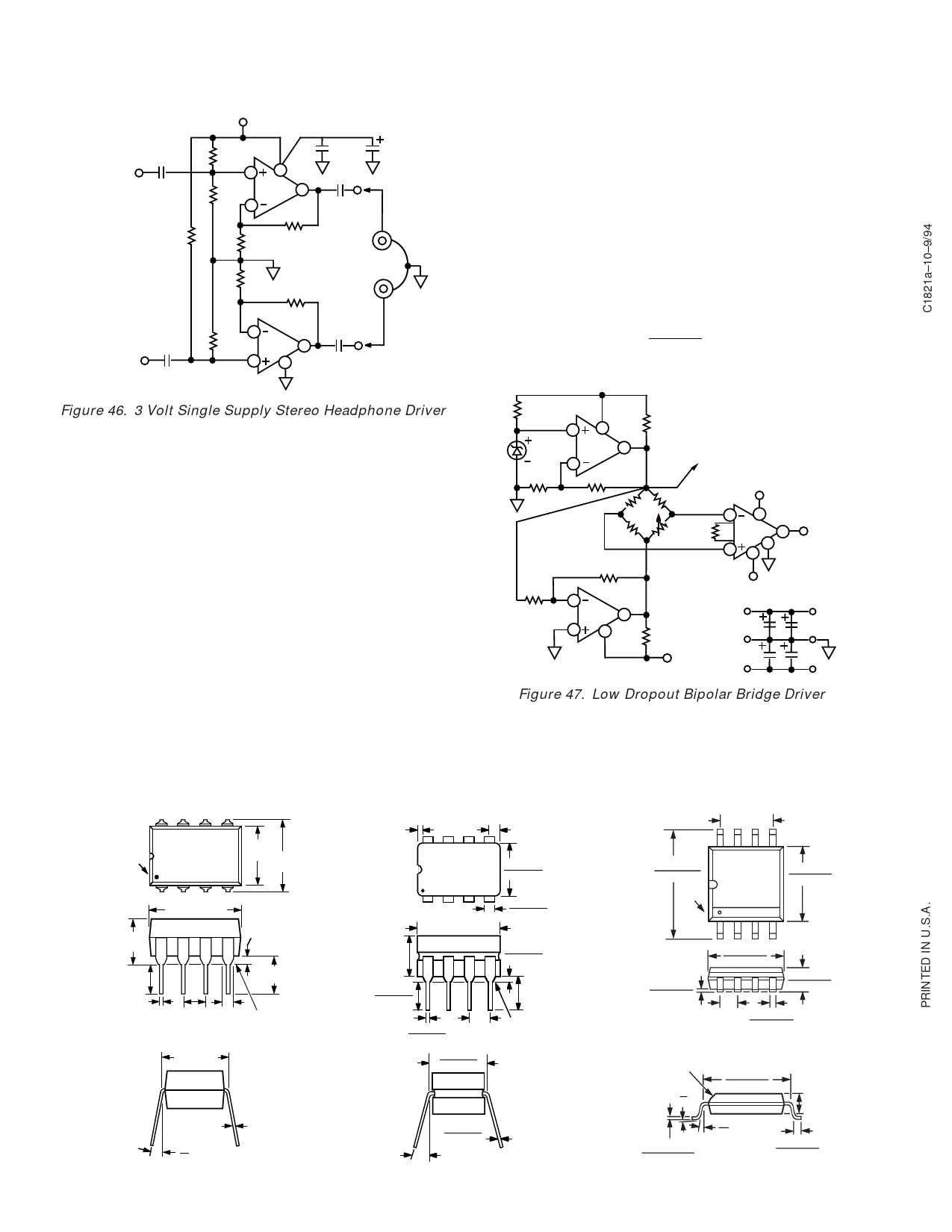
Figure 46. 3 Volt Single Supply Stereo Headphone Driver
3 Volt, Single Supply Stereo Headphone Driver
The AD822 exhibits good current drive and THD+N perfor-
mance, even at 3 V single supplies. At 1 kHz, total harmonic
distortion plus noise (THD+N) equals –62 dB (0.079%) for a
300 mV p-p output signal. This is comparable to other single
supply op amps which consume more power and cannot run on
3 V power supplies.
In Figure 46, each channel s input signal is coupled via a 1 µF
Mylar capacitor. Resistor dividers set the dc voltage at the non-
inverting inputs so that the output voltage is midway between
the power supplies (+1.5 V). The gain is 1.5. Each half of the
AD822 can then be used to drive a headphone channel. A 5 Hz
high-pass filter is realized by the 500 µF capacitors and the head-
phones, which can be modeled as 32 ohm load resistors to
ground. This ensures that all signals in the audio frequency
range (20 Hz–20 kHz) are delivered to the headphones.
Low Dropout Bipolar Bridge Driver
The AD822 can be used for driving a 350 ohm Wheatstone
bridge. Figure 47 shows one half of the AD822 being used to
buffer the AD589—a 1.235 V low power reference. The output
of +4.5 V can be used to drive an A/D converter front end. The
other half of the AD822 is configured as a unity-gain inverter,
and generates the other bridge input of –4.5 V. Resistors R1 and
R2 provide a constant current for bridge excitation. The AD620
low power instrumentation amplifier is used to condition the
differential output voltage of the bridge. The gain of the AD620
is programmed using an external resistor RG, and determined
by:
G = 49.4 kΩ + 1
RG
+VS
49.9k
+1.235V
AD589
10k
3
8
1/2
AD822 1
2
26.4k, 1%
1%
350Ω
350Ω
10k
10k
1%
6
1%
1/2
AD822 7
5
4
R1
20Ω
TO A/D CONVERTER
REFERENCE INPUT
350Ω
350Ω RG
+VS
3
7
AD620 6
2
5
4
–4.5V
R2
20Ω
+VS
VREF
–VS
+VS
0.1µF
GND
0.1µF
–VS
+5V
1µF
1µF
–5V
Figure 47. Low Dropout Bipolar Bridge Driver
Mini-DIP (N) Package
8
PIN 1
1
5
0.25
(6.35) 0.31
(7.87)
4
0.39 (9.91) MAX
0.165±0.01
(4.19±0.25)
0.035±0.01
(0.89±0.25)
0.125
(3.18)
MIN
0.18±0.03
(4.57±0.76)
0.018±0.003
(0.46±0.08)
0.10
(2.54)
BSC
0.033
(0.84)
NOM
SEATING
PLANE
0.30 (7.62)
REF
0.011±0.003
(0.28±0.08)
15°
0°
OUTLINE DIMENSIONS
Dimensions shown in inches and (mm).
Cerdip (Q) Package
0.005 (0.13) MIN
0.055 (1.35) MAX
8
5
1
4
0.405 (10.29) MAX
0.310 (7.87)
0.220 (5.59)
0.070 (1.78)
0.030 (0.76)
0.200
(5.08)
MAX
0.200 (5.08)
0.125 (3.18)
0.060 (1.52)
0.015 (0.38)
0.150
(3.81)
MIN
0.023 (0.58)
0.014 (0.36)
0.100 (2.54)
BSC
SEATING
PLANE
0.320 (8.13)
0.290 (7.37)
0.015 (0.38)
0.008 (0.20)
0°-15°
–16–
SOIC (R) Package
0.150 (3.81)
8
0.244 (6.20)
0.228 (5.79)
PIN 1
1
5
0.157 (3.99)
0.150 (3.81)
4
0.010 (0.25)
0.004 (0.10)
0.197 (5.01)
0.189 (4.80)
0.102 (2.59)
0.094 (2.39)
0.050 0.019 (0.48)
(1.27) 0.014 (0.36)
BSC
0.020 (0.051) x 45°
CHAMF
0.190 (4.82)
8°
0.170 (4.32)
0°
0.090
(2.29)
10°
0°
0.098 (0.2482)
0.075 (0.1905)
0.030 (0.76)
0.018 (0.46)
REV. A
Share Link: 