AD824AR-16 データシートの表示(PDF) - Analog Devices
部品番号
コンポーネント説明
メーカー
AD824AR-16 Datasheet PDF : 16 Pages
| |||
AD824
APPLICATIONS
Single Supply Voltage-to-Frequency Converter
The circuit shown in Figure 31 uses the AD824 to drive a low
power timer, which produces a stable pulse of width t1. The
positive going output pulse is integrated by R1-C1 and used as
one input to the AD824, which is connected as a differential
integrator. The other input (nonloading) is the unknown volt-
age, VIN. The AD824 output drives the timer trigger input, clos-
ing the overall feedback loop.
+10V
C5
0.1µF
U4
REF02
2
6
VREF = 5V
3
5
RSCALE **
10k
4
CMOS
74HCO4
U3B
U3A
4
32
1
C3
0.1µF
R2
499k, 1%
R1
VI N
499k, 1%
0V TO 2.5V
FULL SCALE C2
0.01µF, 2%
0.01µF, 2%
U1
R3*
C1
116k
1/4
AD824B
C6
390pF
5%
(NPO)
U2
CMOS 555
48
6R
THR
2
TR
7
DIS
V+
3
OUT
5
CV
GND
1
C4
0.01µF
OUT2
OUT1
NOTES:
fOUT = VIN /(VREF*t1), t1 = 1.1*R3*C6
= 25kHz fS AS SHOWN.
* = 1% METAL FILM, <50ppm/°C TC
** = 10%, 20T FILM, <100ppm/°C TC
t1 = 33µs FOR fOUT = 20kHz @ VIN = 2.0V
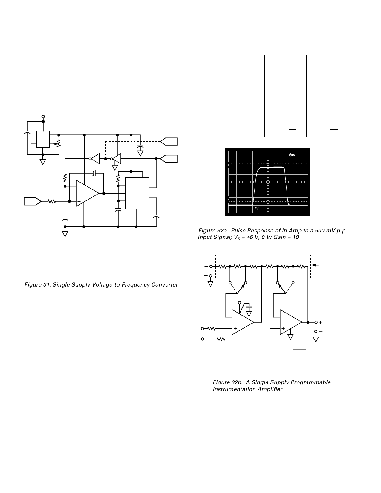
Figure 31. Single Supply Voltage-to-Frequency Converter
Typical AD824 bias currents of 2 pA allow megaohm-range
source impedances with negligible dc errors. Linearity errors on
the order of 0.01% full scale can be achieved with this circuit.
This performance is obtained with a 5 volt single supply, which
delivers less than 3 mA to the entire circuit.
Single Supply Programmable Gain Instrumentation Amplifier
The AD824 can be configured as a single supply instrumenta-
tion amplifier that is able to operate from single supplies down
to 3 V or dual supplies up to ± 15 V. AD824 FET inputs’ 2 pA
bias currents minimize offset errors caused by high unbalanced
source impedances.
An array of precision thin-film resistors sets the in amp gain to
be either 10 or 100. These resistors are laser-trimmed to ratio
match to 0.01% and have a maximum differential TC of
5 ppm/°C.
Table I. AD824 In Amp Performance
Parameters
VS = 3 V, 0 V VS = ؎5 V
CMRR
Common-Mode
Voltage Range
3 dB BW, G = 10
G = 100
tSETTLING
2 V Step (VS = 0 V, 3 V)
5 V (VS = ± 5 V)
Noise @ f = 1 kHz, G = 10
G = 100
74 dB
80 dB
–0.2 V to +2 V –5.2 V to +4 V
180 kHz
180 kHz
18 kHz
18 kHz
2 µs
270 nV/√Hz
2.2 µV/√Hz
5 µs
270 nV/√Hz
2.2 µV/√Hz
5µs
100
90
10
0%
1V
Figure 32a. Pulse Response of In Amp to a 500 mV p-p
Input Signal; VS = +5 V, 0 V; Gain = 10
VREF
R1
R2
R3
R4
R5
R6
90k
9k
1k
1k
9k
90k
OHMTEK
PART # 1043
G =10
G =100 G =100
+VS
0.1µF
G =10
2
6
RP
VIN1
1/4 8 1
3 AD824
1kΩ RP
1/4
7
5 AD824
11
VOUT
VIN2
1kΩ
(G =10)
VOUT
=
(VIN1
–
VIN2)
(1+
R6
R4 + R5
)
+VREF
(G =100)
VOUT
=
(VIN1
–
VIN2 )
(1+
R5 + R6
R4
)
+VREF
FOR R1 = R6, R2 = R5 AND R3 = R4
Figure 32b. A Single Supply Programmable
Instrumentation Amplifier
–12–
REV. A
Share Link: 