AD9898 データシートの表示(PDF) - Analog Devices
部品番号
コンポーネント説明
メーカー
AD9898 Datasheet PDF : 52 Pages
| |||
AD9898
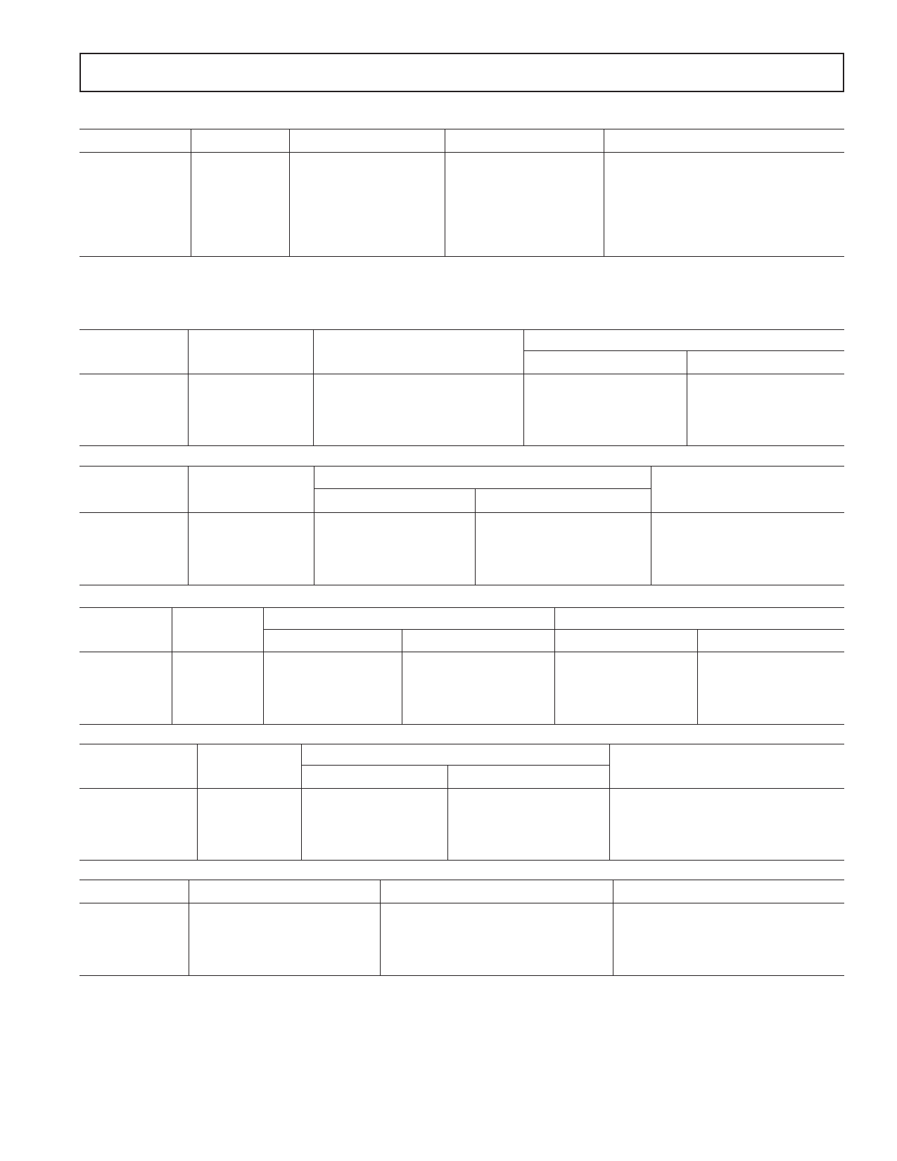
Table VIII. RG, H1, SHP, SHD, DCLK, and DOUTPHASE Timing Parameters
Register Name Bit Width
RGNEGLOC
6
H1POSLOC
6
SHPLOC
6
SHDLOC
6
DOUTPHASE
6
DCLKPHASE
6
The 2 MSB are used to select the quadrant.
Register Type
Control (Addr 0x03)
Control (Addr 0x03)
Control (Addr 0x02)
Control (Addr 0x02)
Control (Addr 0x02)
Control (Addr 0x02)
Range
0–47 Edge Location
0–47 Edge Location
0–47 Edge Location
0–47 Edge Location
0–47 Edge Location
0–47 Edge Location
Description
Falling Edge Location for RG
Positive Edge Location for H1
Sample Location for SHP
Sample Location for SHD
Phase Location of Data Output [9:0]
Positive Edge of DCLK 1
Table IX. Precision Timing Edge Locations for RG, H1, SHP, SHD, DCLK, and DOUTPHASE
Signal Name
RG
Quadrant
I
II
III
IV
RG Rising Edge
(Not Programmable)
Fixed at 000000
Fixed at 000000
Fixed at 000000
Fixed at 000000
RG Falling Edge
RGNEGLOC
Quadrant Range
000000 to 001011
010000 to 011011
100000 to 101011
110000 to 111011
P[0] to P[11]
P[12] to P[23]
P[24] to P[35]
P[36] to P[47]
Signal Name
H1
Quadrant
I
II
III
IV
H1 Rising Edge
H1POSLOC
Quadrant Range
000000 to 001011
010000 to 011011
100000 to 101011
110000 to 111011
P[0] to P[11]
P[12] to P[23]
P[24] to P[35]
P[36] to P[47]
H1 Falling Edge
(Not Programmable)
H1POSLOC + 24 Steps
H1POSLOC + 24 Steps
H1POSLOC + 24 Steps
H1POSLOC + 24 Steps
Signal Name
cds
Quadrant
I
II
III
IV
cds Rising Edge
SHPLOC
Quadrant Range
000000 to 001011
010000 to 011011
100000 to 101011
110000 to 111011
P[0] to P[11]
P[12] to P[23]
P[24] to P[35]
P[36] to P[47]
cds Falling Edge
SHDLOC
Quadrant Range
000000 to 001011
010000 to 011011
100000 to 101011
110000 to 111011
P[0] to P[11]
P[12] to P[23]
P[24] to P[35]
P[36] to P[47]
Signal Name
Data Output[9:0]
Quadrant
I
II
III
IV
Data Output[9:0] Rising Edge
DOUTPHASE
Quadrant Range
000000 to 001011
010000 to 011011
100000 to 101011
110000 to 111011
P[0] to P[11]
P[12] to P[23]
P[24] to P[35]
P[36] to P[47]
Data Output[9:0] Falling Edge
(Not Programmable)
DOUTPHASE + 24 Steps
DOUTPHASE + 24 Steps
DOUTPHASE + 24 Steps
DOUTPHASE + 24 Steps
Signal Name
DCLK1
DCLKPHASE Value
00
01
10
11
DCLKPHASE Rising Edge
P[6]
P[16]
P[26]
P[36]
DCLKPHASE Falling Edge
P[26]
P[36]
P[06]
P[16]
REV. 0
–21–
Share Link: 