ADF4153BRU-REEL7(RevA) データシートの表示(PDF) - Analog Devices
部品番号
コンポーネント説明
メーカー
ADF4153BRU-REEL7 Datasheet PDF : 24 Pages
| |||
PHASE FREQUENCY DETECTOR (PFD) AND
CHARGE PUMP
The PFD takes inputs from the R counter and N counter and
produces an output proportional to the phase and frequency
difference between them. Figure 19 is a simplified schematic.
The PFD includes a fixed delay element that sets the width of
the antibacklash pulse, which is typically 3 ns. This pulse
ensures that there is no dead zone in the PFD transfer function,
and gives a consistent reference spur level.
HI
+IN
UP
D1 Q1
U1
CLR1
DELAY U3
CHARGE
CP
PUMP
HI
–IN
CLR2 DOWN
D2 Q2
U2
Figure 19. PFD Simplified Schematic
MUXOUT AND LOCK DETECT
The output multiplexer on the ADF4153 allows the user to
access various internal points on the chip. The state of
MUXOUT is controlled by M3, M2, and M1 (see Table 8).
Figure 20 shows the MUXOUT section in block diagram form.
The N-channel open-drain analog lock detect should be
operated with an external pull-up resistor of 10 kΩ nominal.
When lock has been detected, it is high with narrow low-going
pulses.
DVDD
THREE-STATE OUTPUT
LOGIC LOW
DIGITAL LOCK DETECT
R COUNTER OUTPUT
N COUNTER OUTPUT
ANALOG LOCK DETECT
LOGIC HIGH
MUX
CONTROL
MUXOUT
Figure 20. MUXOUT Schematic
DGND
ADF4153
INPUT SHIFT REGISTERS
The ADF4153 digital section includes a 4-bit RF R counter, a 9-
bit RF N counter, a 12-bit FRAC counter, and a 12-bit modulus
counter. Data is clocked into the 24-bit shift register on each
rising edge of CLK. The data is clocked in MSB first. Data is
transferred from the shift register to one of four latches on the
rising edge of LE. The destination latch is determined by the
state of the two control bits (C2 and C1) in the shift register.
These are the 2 LSBs, DB1 and DB0, as shown in Figure 2. The
truth table for these bits is shown in Table 5. Table 6 shows a
summary of how the latches are programmed.
PROGRAM MODES
Table 5 through Table 10 show how to set up the program
modes in the ADF4153.
The ADF4153 programmable modulus is double buffered. This
means that two events have to occur before the part uses a new
modulus value. First, the new modulus value is latched into the
device by writing to the R divider register. Second, a new write
must be performed on the N divider register. Therefore, any
time that the modulus value has been updated, the N divider
register must be written to after this, to ensure that the modulus
value is loaded correctly.
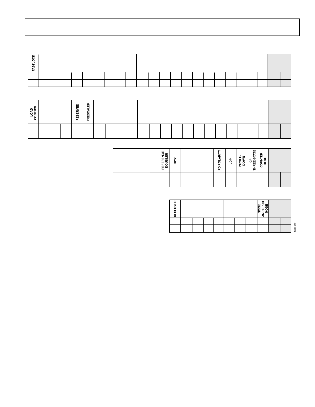
Table 5. C2 and C1 Truth Table
Control Bits
C2
C1
Register
0
0
N Divider Register
0
1
R Divider Register
1
0
Control Register
1
1
Noise and Spur Register
Rev. A | Page 11 of 24
Share Link: 