ATA6602 データシートの表示(PDF) - Atmel Corporation
部品番号
コンポーネント説明
メーカー
ATA6602 Datasheet PDF : 362 Pages
| |||
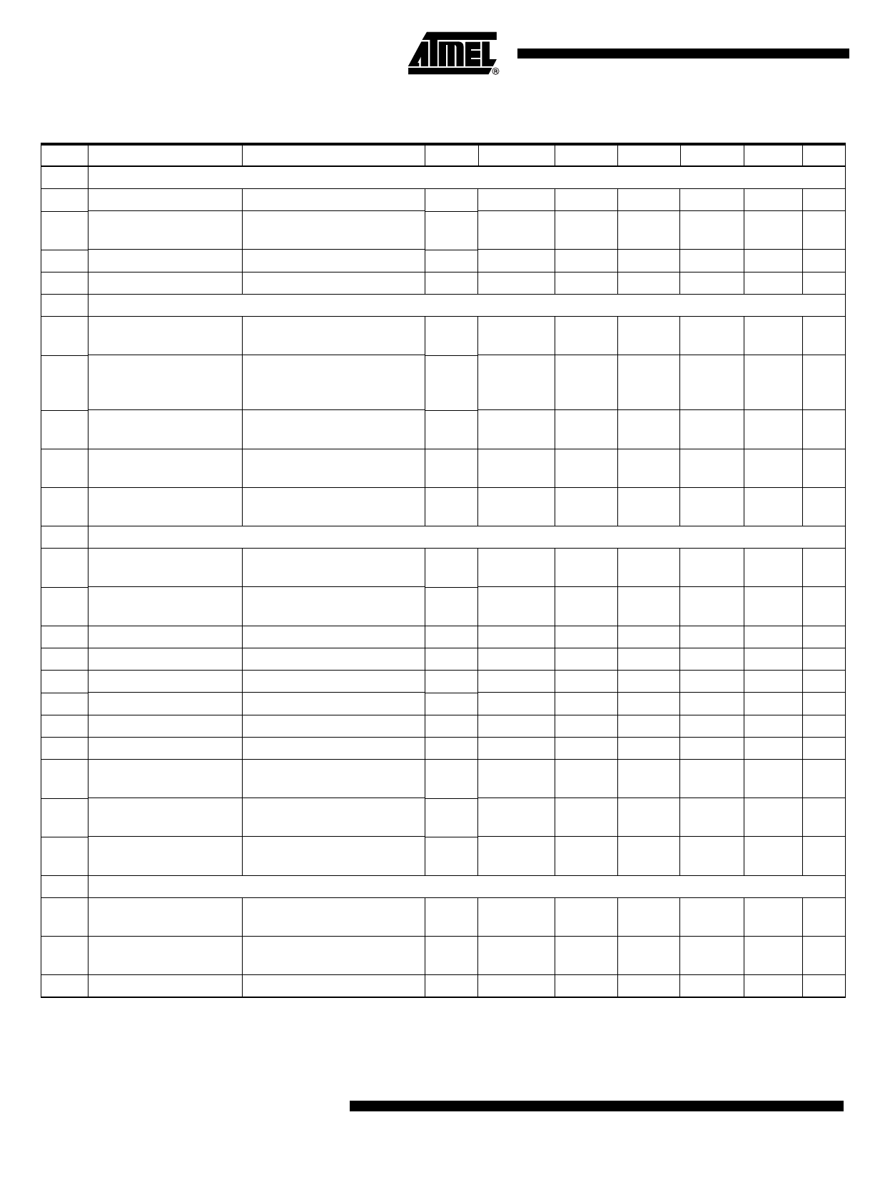
3.5 Electrical Characteristics (Continued)
5V < VS < 18V, Tcase = –40°C to +125°C
No. Parameters
Test Conditions
Pin Symbol Min.
Typ.
Max.
4 EN Input Pin
4.1 Low-level voltage input
4.2 High-level voltage input
29
VENL
–0.3
29
VENH
3.5
+1.5
VDD +
0.3V
4.3 Pull-down resistor
4.4 Low-level input current
5 NRES Output Pin
VEN = 5V
VEN = 0V
29
REN
125
250
600
29
IEN
–3
+3
5.1
High-level output voltage
VS ≥ 5.5V;
Inres = –1 mA
21
VNRESH
4.5
VS ≥ 5.5V;
5.2 Low-level output voltage Inres = –1 mA,
Inres = –250 µA
21
VNRESL
5.3 Low-level output low
10 kΩ to VDD;
VDD = 0.8V
21
VNRESLL
5.4
Undervoltage reset time
VVS ≥ 5.5V
CNRES = 20 pF
21
treset
7
5.5
Reset debounce time for VVS ≥ 5.5V
falling edge
CNRES = 20 pF
21
tres_f
6 Voltage Regulator VDD Pin in Normal and Pre Normal Mode
0.2
0.14
0.3
13
3
6.1 Output voltage VDD
5.5V < VS < 18V
(0 mA to 50 mA)
27
VDDnor
4.9
5.1
6.2
Output voltage VDD at
low VS
3.3V < VS < 5.5V
6.3 Regulator drop voltage VS > 4.0V, IVDD = –20 mA
6.4 Regulator drop voltage VS > 4.0V, IVDD = –50 mA
6.5 Regulator drop voltage VS > 3.3V, IVDD = –15 mA
6.6 Output current
VS > 3V
6.7 Output current limitation VS > 0V
6.8 Load capacity
1Ω < ESR < 5Ω
6.9
VDD undervoltage
threshold
Referred to VDD
VS > 5.5V
6.10
Hysteresis of
undervoltage threshold
Referred to VDD
VS > 5.5V
6.11
Ramp up time VS > 5.5V CVDD = 4.7 µF
to VDD > 4.9V
No load
27
VDDlow
VVS
– VD
5.1
27
VD1
250
27
VD2
500
27
VD3
200
27
IVDD
–50
27
IVDDs
–200 –130
27
Cload
1.8
2.2
27
VthunN
4.4
4.8
27
Vhysthun
30
27
tVDD
300
7 Voltage Regulator VDD Pin in Silent Mode
7.1 Output voltage VDD
5.5V < VS < 18V
(0 mA to 50 mA)
27
VDDnor
4.65
5.35
7.2
Output voltage VDD at
low VS
3.3V < VS < 5.5V
27
VDDlow
VVS
– VD
5.1
7.3 Regulator drop voltage VS > 3.3V, IVDD = –15 mA
27
VD
200
*) Type means: A = 100% tested, B = 100% correlation tested, C = Characterized on samples, D = Design parameter
Unit Type*
V
A
V
A
kΩ
A
µA
A
V
A
V
A
V
A
V
A
ms
A
µs
A
V
A
V
A
mV
A
mV
A
mV
A
mA
A
mA
A
µF
D
V
A
mV
A
µs
A
V
A
V
A
mV
A
20 ATA6602/ATA6603
4921C–AUTO–01/07
Share Link: 