ATA6620N データシートの表示(PDF) - Atmel Corporation
部品番号
コンポーネント説明
メーカー
ATA6620N Datasheet PDF : 22 Pages
| |||
ATA6620N
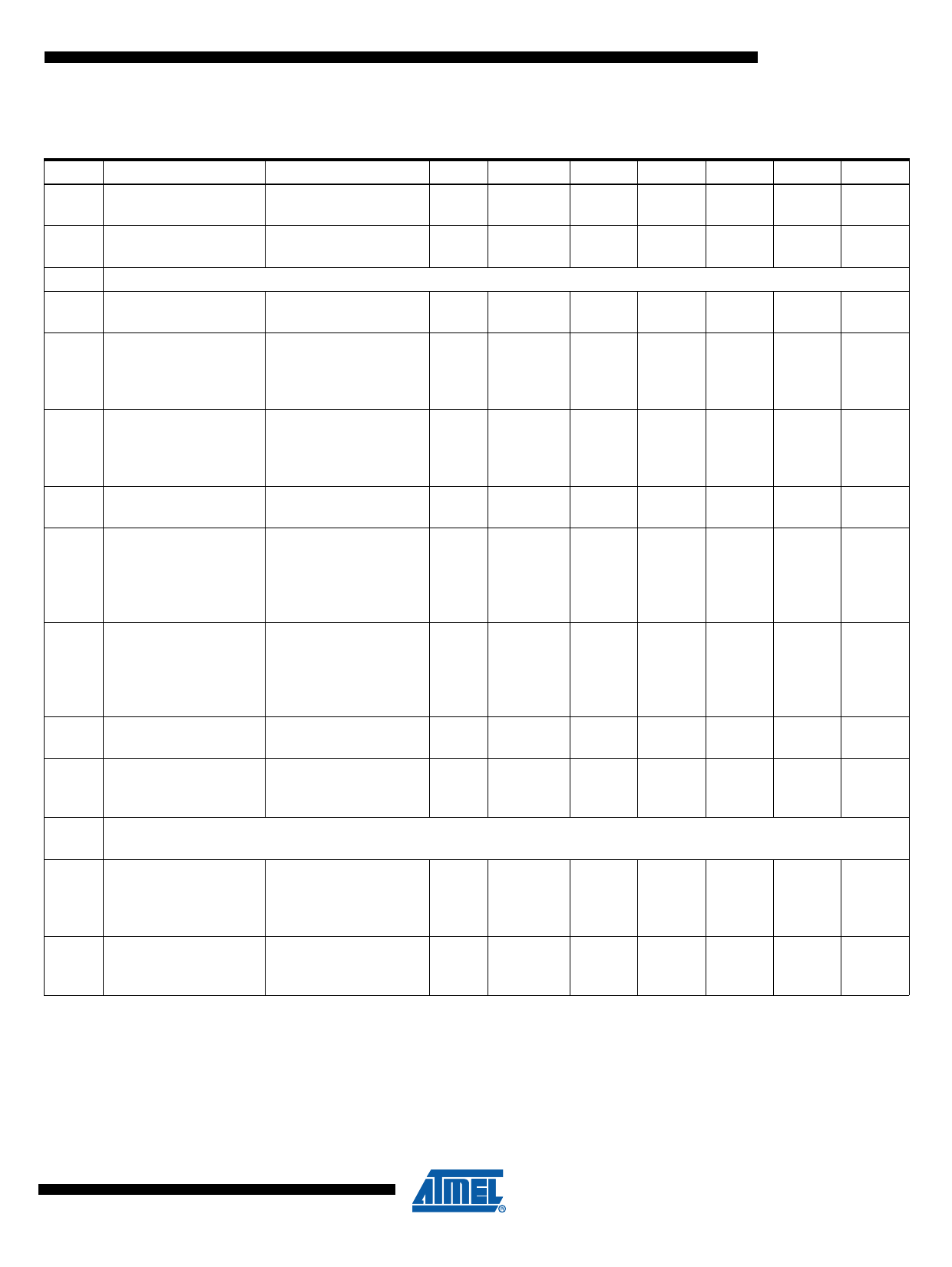
8. Electrical Characteristics (Continued)
5V < VS < 18V, Tamb = –40°C to 125°C
No. Parameters
Test Conditions
Pin Symbol Min.
Typ.
Max.
Unit
9.5
Wake detection LIN
High level input voltage
LIN
VLINH
VS – 1V
VS + 0.3V V
9.6
Wake detection LIN
Low level input voltage
ILIN = typically –3 mA
LIN
VLINL
–27
VS – 3.3V V
10 Internal Timers
10.1
Dominant time for
wake–up via LIN bus
VLIN = 0V
tbus
30
90
150
µs
Time delay for mode
10.2
change from Pre-normal
into Normal mode via
VEN = 5V
pin EN
tnorm
5
20
µs
Time delay for mode
10.3
change from Normal
mode to Sleep mode via
VEN = 0V
pin EN
tsleep
2
7
15
µs
10.4
TXD dominant time out
timer
VTXD = 0V
tdom
6
10
20
ms
10.5
10.6
10.7
10.8
Duty cycle 1
Duty cycle 2
Slope time falling and
rising edge at LIN
THRec(max) = 0.744 × VS;
THDom(max) = 0.581 × VS;
VS = 7.0V to 18V;
tBit = 50 ms
D1 = tbus_rec(min)/(2 × tBit)
THRec(min) = 0.422 × VS;
THDom(min) = 0.284 × VS;
VS = 7.0V to 18V;
tBit = 50ms
D2 = tbus_rec(max)/(2 × tBit)
Time delay for mode
change from Silent- into VEN = 5V
Normal mode via EN
D1
0.396
D2
0.581
tSLOPE_fall
tSLOPE_rise
3.5
ts_n
5
22.5
µs
15
40
µs
11
11.1
Receiver Electrical AC Parameters of the LIN Physical Layer
LIN Receiver, RXD Load Conditions (CRXD): 20 pF; Rpull-up = 2.4 kΩ
Propagation delay of
receiver Switch to Sleep
mode (see Figure 8-1 on
trx_pd = max(trx_pdr, trx_pdf)
trx_pd
page 18)
6
µs
11.2
Symmetry of receiver
propagation delay rising trx_sym = trx_pdr – trx_pdf
edge minus falling edge
trx_sym
–2
+2
µs
*) Type means: A = 100% tested, B = 100% correlation tested, C = Characterized on samples, D = Design parameter
Type*
A
A
A
A
A
A
A
A
A
A
A
A
17
4850I–AUTO–09/09
Share Link: 