ATTINY20 データシートの表示(PDF) - Atmel Corporation
部品番号
コンポーネント説明
メーカー
ATTINY20 Datasheet PDF : 219 Pages
| |||
The first 64 locations are reserved for I/O memory, while the following 128 data memory locations (from 0x0040 to
0x00BF) address the internal data SRAM.
The non-volatile memory lock bits and all the Flash memory sections are mapped to the data memory space. These
locations appear as read-only for device firmware.
The four different addressing modes for data memory are direct, indirect, indirect with pre-decrement, and indirect with
post-increment. In the register file, registers R26 to R31 function as pointer registers for indirect addressing.
The IN and OUT instructions can access all 64 locations of I/O memory. Direct addressing using the LDS and STS
instructions reaches the 128 locations between 0x0040 and 0x00BF.
The indirect addressing reaches the entire data memory space. When using indirect addressing modes with automatic
pre-decrement and post-increment, the address registers X, Y, and Z are decremented or incremented.
5.2.1
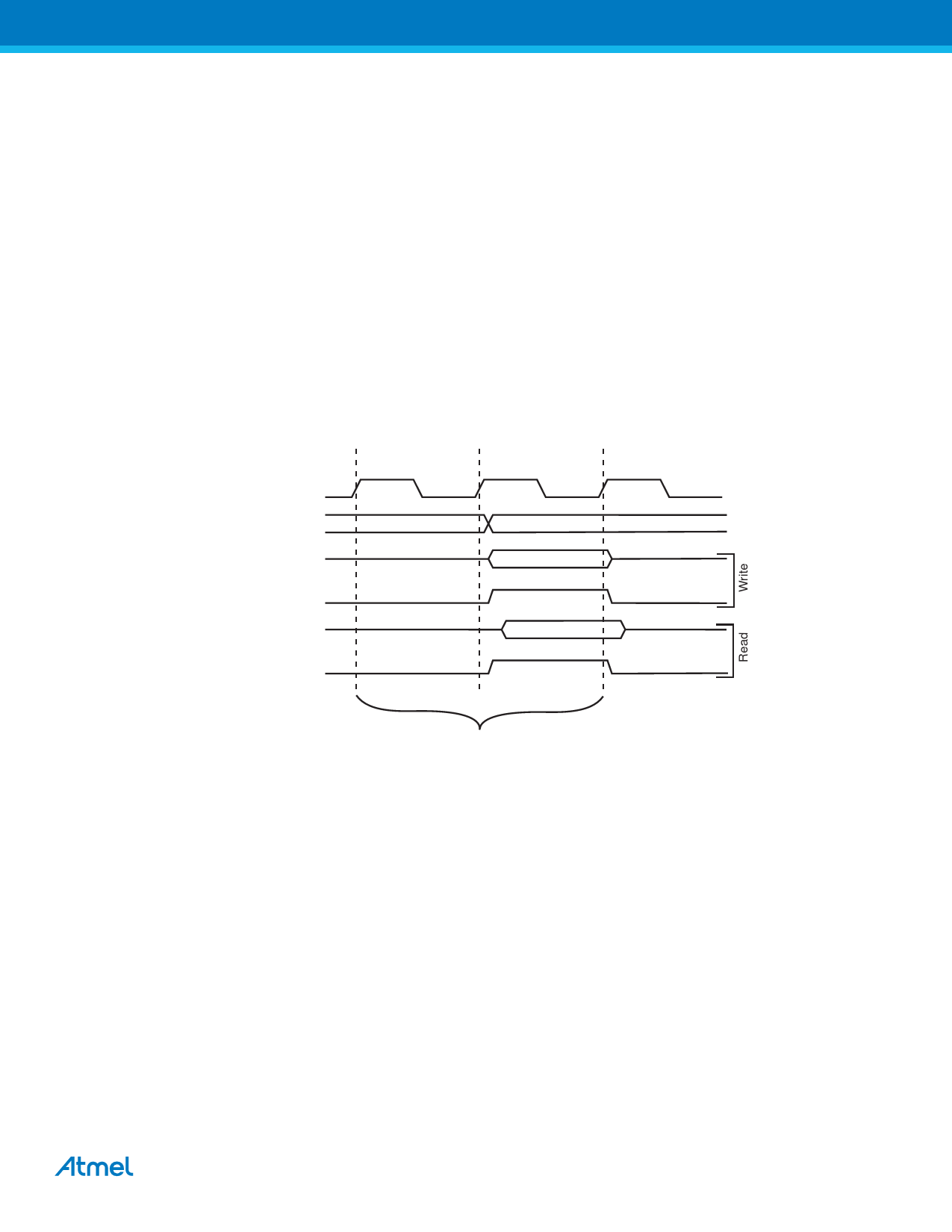
Data Memory Access Times
This section describes the general access timing concepts for internal memory access. The internal data SRAM access
is performed in two clkCPU cycles as described in Figure 5-2.
Figure 5-2. On-chip Data SRAM Access Cycles
T1
T2
T3
clk
CPU
Address
Data
WR
Data
RD
Compute Address
Address valid
Memory Access Instruction
Next Instruction
5.3 I/O Memory
The I/O space definition of the ATtiny20 is shown in “Register Summary” on page 203.
All ATtiny20 I/Os and peripherals are placed in the I/O space. All I/O locations may be accessed using the LD and ST
instructions, enabling data transfer between the 16 general purpose working registers and the I/O space. I/O Registers
within the address range 0x00 - 0x1F are directly bit-accessible using the SBI and CBI instructions. In these registers, the
value of single bits can be checked by using the SBIS and SBIC instructions. See document “AVR Instruction Set” and
section “Instruction Set Summary” on page 205 for more details. When using the I/O specific commands IN and OUT, the
I/O addresses 0x00 - 0x3F must be used.
For compatibility with future devices, reserved bits should be written to zero if accessed. Reserved I/O memory
addresses should never be written.
Some of the status flags are cleared by writing a logical one to them. Note that CBI and SBI instructions will only operate
on the specified bit, and can therefore be used on registers containing such status flags. The CBI and SBI instructions
work on registers in the address range 0x00 to 0x1F, only.
The I/O and Peripherals Control Registers are explained in later sections.
ATtiny20 [DATASHEET] 16
Atmel-8235F-AVR-ATtiny20-Datasheet_09/2014
Share Link: 