TC820CLW データシートの表示(PDF) - TelCom Semiconductor Inc => Microchip
部品番号
コンポーネント説明
メーカー
TC820CLW
TelCom Semiconductor Inc => Microchip

TC820CLW Datasheet PDF : 22 Pages
| |||
3-3/4 A/D CONVERTER WITH
FREQUENCY COUNTER
AND LOGIC PROBE
1
TC820
9V +
22kΩ
VSS VDD
VR+EF 2kΩ
TC820
VREF
VR–EF
ANALOG
COMMON
SET VREF = 1/2 VFULL SCALE
(a) Internal Reference
V+
2kΩ
VDD
TC820
VR+EF
VR–EF
COMMON
TC04A
1.2V
REF
(b) External Reference
+
1µF
+9V
2
TC820
VDD
DGND
FREQ/VOLTS
FREQUENCY
INPUT
74HC14
RANGE/FREQ
3
GND
DGND
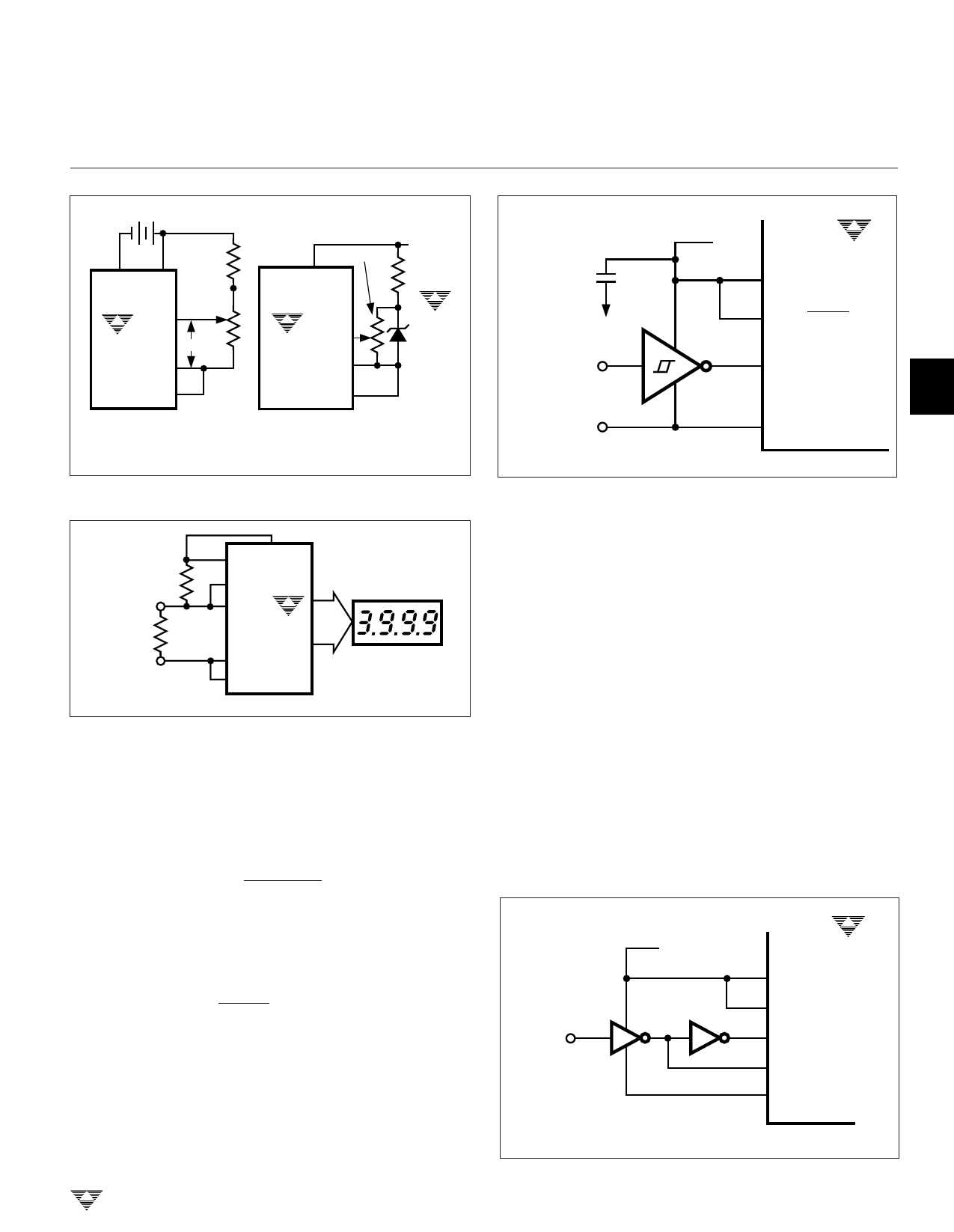
Figure 18. Reference Voltage Connections
Figure 20. Frequency Counter External Buffer
RSTANDARD
RUNKNOWN
VR+EF VDD
VR–EF
VI+N
TC820
VI–N
ANALOG
COMMON
LCD
Figure 19. Low Parts Count Ratiometric Resistance Measurement
applied to the reference input. If the unknown equals the
standard, the input voltage will equal the reference voltage
and the display will read 2000. The displayed reading can be
determined from the following expression:
RUNKNOWN
Displayed reading =
ϫ 2000
RSTANDARD
The display will overrange for values of RUNKNOWN ≥ 2
ϫ RSTANDARD.
Buffering the FREQ Input
When the FREQ/VOLTS input is high and the LOGIC
input is low, the TC820 will count pulses at the RANGE/
FREQ input. The time base will be fOSC/40,000, or 1 second
with a 40kHz clock. The signal to be measured should swing
from VDD to DGND. The RANGE/FREQ input has CMOS
input levels without hysteresis. For best results, especially
with low-frequency sine-wave inputs, an external buffer with
hysteresis should be added. A typical circuit is shown in
Figure 20.
TELCOM SEMICONDUCTOR, INC.
Logic Probe Inputs
4
The DP0/LO and DP1/HI inputs provide the logic probe
inputs when the LOGIC input is high. Driving either DP0/LO
or DP1/HI to a logic high will turn on the appropriate LCD
annunciator. When DP0/LO is high, the buzzer will be on.
To provide a "single input" logic probe function, external
buffers should be used. A simple circuit is shown in Figure
5 21. This circuit will turn the appropriate annunciator on for
high and low level inputs.
If carefully controlled logic thresholds are required, a
window comparator can be used. Figure 22 shows a typical
circuit. This circuit will turn on the high or low annunciators
when the logic thresholds are exceeded, but the resistors
connected from DP0/LO and DP1/HI to DGND will turn both
annunciators off when the logic probe is unconnected.
6 The TC820 logic inputs are not latched internally, so
pulses of short duration will usually be difficult or impossible
to see. To display short pulses properly, the input pulse
should be "stretched." The circuit of Figure 22 shows cap-
+9V
LOGIC
PROBE
INPUT
*
*
* 74HC14
TC820
VDD
LOGIC
DP1/HI
DP0/LO
DGND
Figure 21. Simple External Logic Probe Buffer
7
8
3-167
Share Link: