BA4510F データシートの表示(PDF) - ROHM Semiconductor
部品番号
コンポーネント説明
メーカー
BA4510F Datasheet PDF : 51 Pages
| |||
BA4558F,BA4558R F/FV/FVM,BA4560F,BA4560RF/FV/FVM,BA4564RFVBA4580RF/FVM,BA4584FV,
BA4584RF/FV,BA8522RF/FV/FVM,BA15218F,BA14741F,BA15532F,BA4510F/FV,BA2115F/FVM
Technical Note
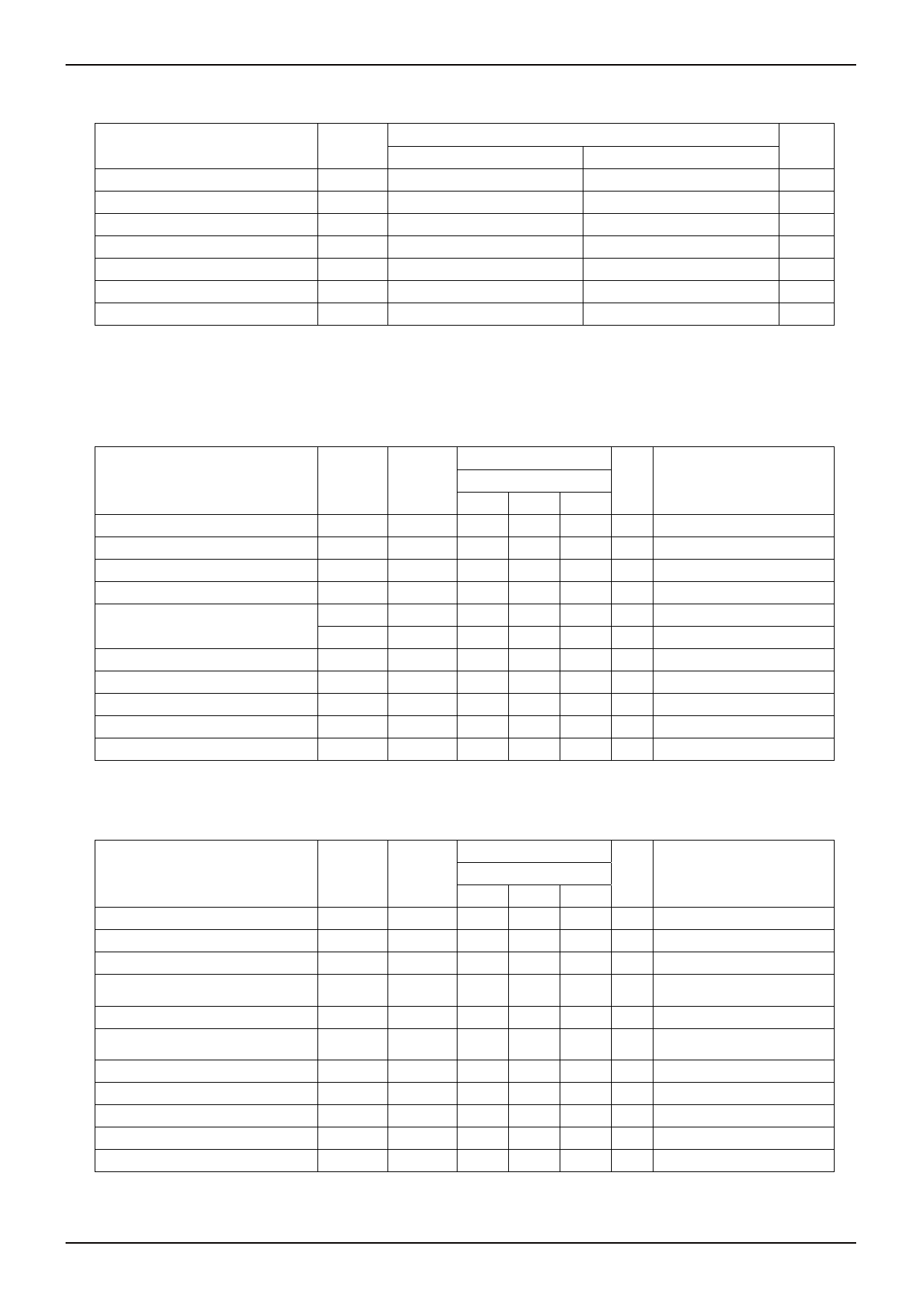
●Absolute maximum rating (Ta=25[℃])
○BA4510/BA2115 family
Parameter
Symbol
BA4510 family
Ratings
BA2115 family
Supply Voltage
VCC-VEE
10
14
Differential Input Voltage (*32)
Vid
VCC-VEE
14
Input Common-mode Voltage Range Vicm
VEE~VCC
(VEE-0.3)~VEE+14
Operating Supply Voltage
Vopr
2~7(±1~±3.5)
2~14(±1~±7)
Operating Temperature
Topr
-20~+75
-40~+85
Storage Temperature
Tstg
-40~125
-55~150
Maximum Junction Temperature Tjmax
125
150
Note: Absolute maximum rating item indicates the condition which must not be exceeded.
Application of voltage in excess of absolute maximum rating or use out absolute maximum rated temperature environment may cause
deterioration of characteristics.
(*32) The voltage difference between inverting input and non-inverting input is the differential input voltage.
Then input terminal voltage is set to more than VEE.
Unit
V
V
V
V
℃
℃
℃
●Electrical characteristics
○BA4510 family (Unless otherwise specified VCC=+2.5[V], VEE=-2.5[V], Ta=25[℃])
Parameter
Limits
Symbol
Temperature
Range
BA4510F/FV
Unit
Min. Typ. Max.
Input Offset Voltage (*33)
Vio
25℃
-
1
6 mV
Input Offset Current (*33)
Iio
25℃
-
2
200 nA
Input Bias Current (*34)
Ib
25℃
-
80 500 nA
Supply Current
ICC
25℃
2.5 5.0 7.5 mA
Maximum Output Voltage
VOH
VOL
25℃
25℃
+2.0 +2.4
-
V
-
-2.4 -2.0 V
Large Signal Voltage Gain
Av
25℃
60
90
-
dB
Input Common-mode Voltage Range Vicm
25℃ -1.3
-
+1.5 V
Common-mode Rejection Ratio
CMRR 25℃
60
80
-
dB
Power Supply Rejection Ratio
PSRR
25℃
60
80
-
dB
Slew Rate
SR
25℃
-
5.0
- V/μs
(*33) Absolute value
(*34) Current direction: Since first input stage is composed with PNP transistor, input bias current flows out of IC.
Condition
Rs=50[Ω]
RL=∞ All Op-Amps
RL=10[kΩ]
RL=10[kΩ]
RL≧10[kΩ]
Rs=50[Ω]
Av=1
●Electrical characteristics
○BA2115 family (Unless otherwise specified VCC=+2.5[V], VEE=-2.5[V], Ta=25[℃])
Parameter
Limits
Symbol
Temperature
Range
BA2115F/FVM
Unit
Min. Typ. Max.
Input Offset Voltage (*35)
Vio
25℃
-
1
6 mV
Input Offset Current (*35)
Iio
25℃
-
2
200 nA
Input Bias Current (*36)
Ib
25℃
-
150 400 nA
Supply Current
ICC
25℃
-
3.5
5 mA
Maximum Output Voltage
VOM
25℃ ±2.0 ±2.2
-
V
Large Signal Voltage Gain
AV
25℃
60
80
-
dB
Input Common-mode Voltage Range Vicm
25℃ ±1.5
-
-
V
Common-mode Rejection Ratio
CMRR
25℃
60
74
-
dB
Power Supply Rejection Ratio
PSRR
25℃
60
80
-
dB
Slew Rate
SR
25℃
-
4
- V/μs
Gain Bandwidth Product
GB
25℃
-
12
- MHz
(*35) Absolute value
(*36) Current direction: Since first input stage is composed with PNP transistor, input bias current flows out of IC.
Condition
VOUT=0[V], Vicm=0[V]
VOUT=0[V], Vicm=0[V]
VOUT=0[V], Vicm=0[V]
RL=∞ All Op-Amps,
VIN+=0[V]
RL≧2.5[kΩ]
RL≧10[kΩ],
VOUT=±2[V], Vicm=0[V]
Vicm=-1.5[V]~+1.5[V]
VCC=+2[V]~+14[V]
AV=0[dB], VIN=±1[V]
f=10[kHz]
www.rohm.com
© 2011 ROHM Co., Ltd. All rights reserved.
12/48
2011.08 - Rev.B
Share Link: 