BGX7101 データシートの表示(PDF) - NXP Semiconductors.
部品番号
コンポーネント説明
メーカー
BGX7101 Datasheet PDF : 40 Pages
| |||
NXP Semiconductors
12. Application information
BGX7101
Transmitter IQ modulator
100 nF
VCC
22 pF
modulator in-phase
positive input
modulator in-phase
negative input
24
POFF_P
1
LO input
1
5
O PRIMARY O
TC1-1-43A+
3
4
LOGND 2
18 pF LO_P 3
0.3 pF
LO_N 4
18 pF
LOGND 5
LOGND
6
7
23
22
21
20
19
VCC_RF(5V0)
18
VCC
BGX7101
RFGND
17
22 pF
100 nF
0°
90°
8
9
10
16 RFOUT
39 pF
RFOUTPUT
0.4 pF
15 i.c.
14 RFGND
13 i.c.
11
12
modulator quadrature
negative input
modulator quadrature
positive input
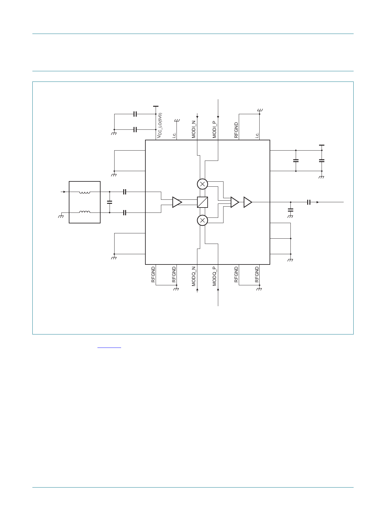
Fig 4. Typical wideband application diagram
aaa-002966
Figure 4 shows a typical wideband (from 0.4 GHz to 4 GHz) application circuit. Refer to
the application note for narrowband optimum component values.
12.1 External DAC interfacing
Nominal DAC single-ended output currents are between 0 mA to 20 mA. When driving
into 25 impedance, this creates 250 mV peak-single signal (1 V (p-p) differential). Half
of the impedance is placed at the DAC outputs as 50 load resistors, the other half is
provided by the modulator itself. In this way, the differential filter can be properly
terminated by 100 at both ends.
BGX7101
Product data sheet
All information provided in this document is subject to legal disclaimers.
Rev. 5 — 25 January 2017
© NXP B.V. 2017. All rights reserved.
12 of 40
Share Link: 