LCX007BNB データシートの表示(PDF) - Sony Semiconductor
部品番号
コンポーネント説明
メーカー
LCX007BNB Datasheet PDF : 24 Pages
| |||
LCX007BNB
[Description of operating mode]
The LCD panel has the following functions to easily apply to various uses, as well as various broadcasting
systems.
• Right/left inverse mode
• Up/down inverse mode
• 4:3 display mode with side-black display
These modes are controlled by three signals (RGT, DWN, and WID). The setting mode is shown below:
WID RGT
Mode
H H 16:9 right scan
H L 16:9 left scan
L H 4:3 right scan
L L 4:3 left scan
DWN
Mode
H Down scan
L Up scan
The direction of the right/left and/or up/down mean when Pin 1 marking is located at right side with the pin
block upside.
• The analog signal (SID) to display side-black shall be input by 1H inversion synchronized with the signal.
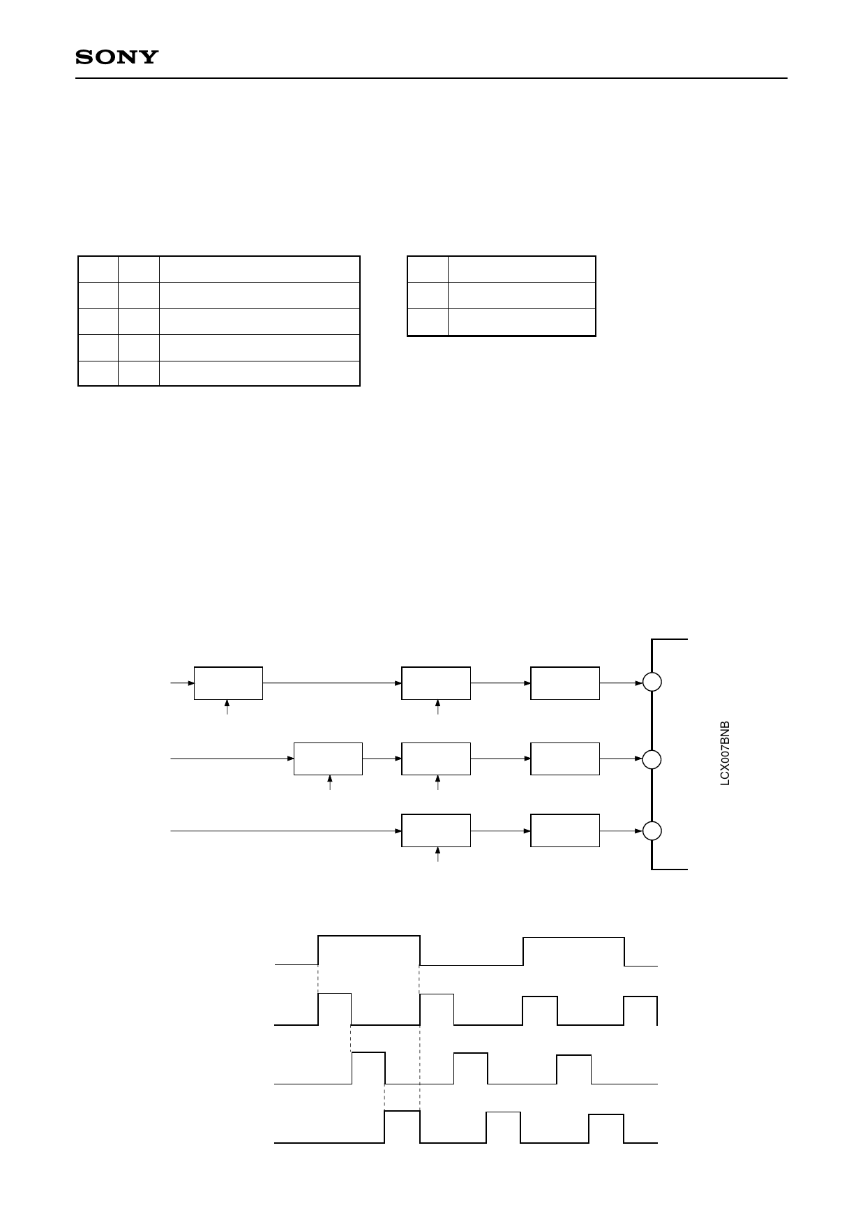
3. 3-dot Simultaneous Sampling
Horizontal driver samples SIG1, SIG2 and SIG3 signal simultaneously, which requires the phase matching
between SIG1, SIG2, and SIG3 signals to prevent horizontal resolution from deteriorating. Thus phase
matching between each signal is required using an external signal delaying circuit before applying video
signal to the LCD panel.
The block diagram of the delaying procedure using sample-and-hold method is as follows.
The LCX007 has the right/left inverse function. The following phase relationship diagram indicates the phase
setting for the right scan (RGT = High level). For the left scan (RGT = Low level), the phase setting shall be
inverted between SIG2 and SIG3 signals.
SIG2
SIG1
SIG3
S/H
S/H
AC Amp
3 SIG2
CK2
CK3
S/H
S/H
AC Amp
2 SIG1
CK1
CK3
S/H
AC Amp
4 SIG3
CK3
<Phase relationship of delaying sample-and-hold pulses> (right scan)
HCKn
CK2
CK1
CK3
– 19 –
Share Link: 