CS61577-IL1Z データシートの表示(PDF) - Cirrus Logic
部品番号
コンポーネント説明
メーカー
CS61577-IL1Z Datasheet PDF : 30 Pages
| |||
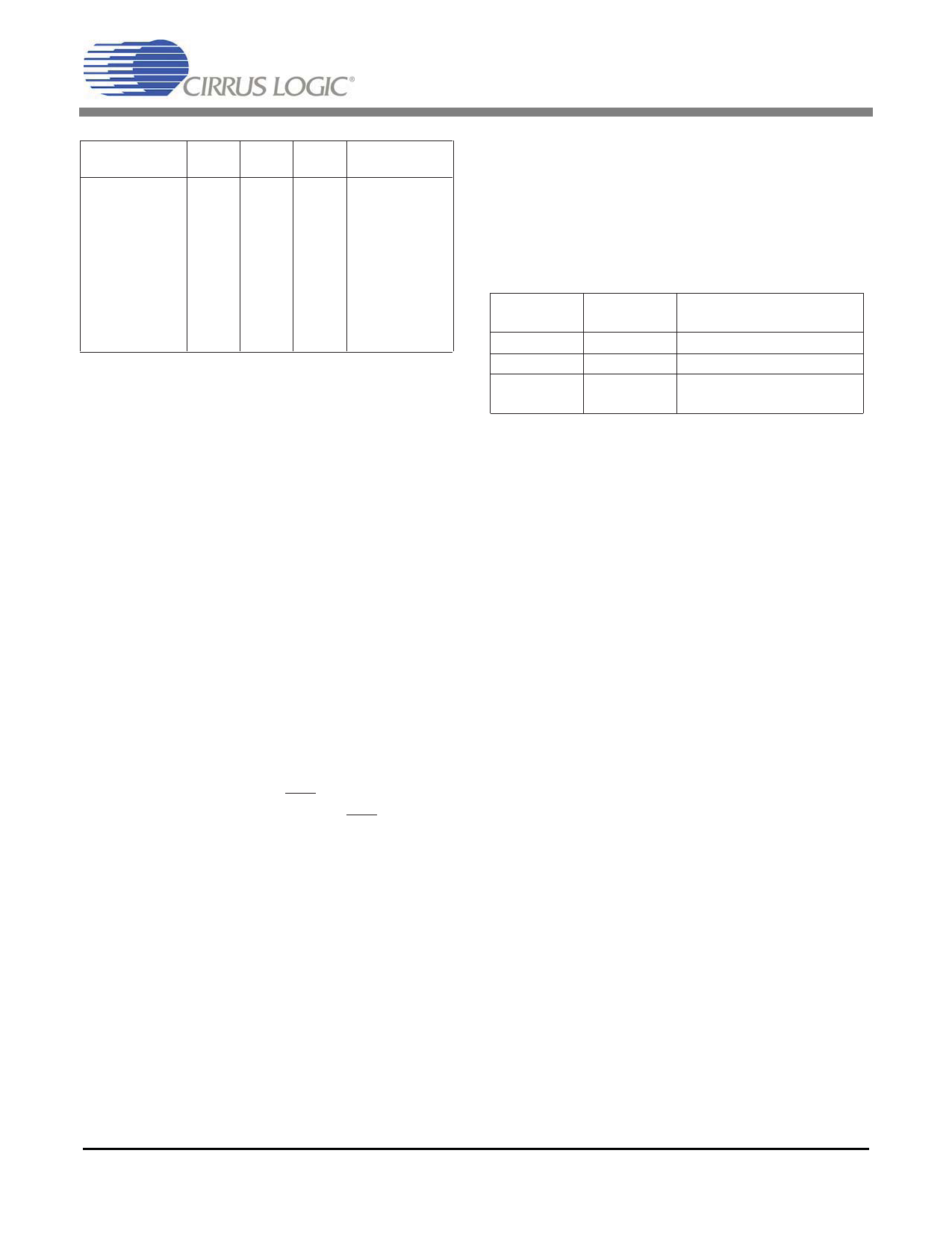
CS61577
#3
MODE
(pin 5)
CLKE
(pin 28) DATA CLOCK
LOW
(<0.2V)
X
RPOS RCLK
RNEG RCLK
HIGH
(>(V+) - 0.2V)
LOW
RPOS
RNEG
SDO
RCLK
RCLK
SCLK
HIGH
(>(V+) - 0.2V)
HIGH
RPOS
RNEG
SDO
RCLK
RCLK
SCLK
MIDDLE
(2.5V)
X RDATA RCLK
X = Don’t Care
Clock Edge for
Valid Data
Rising
Rising
Rising
Rising
Falling
Falling
Falling
Rising
Falling
Table 5. Data Output/Clock Relationship
Loss of Signal
The receiver will indicate loss of signal after
power-up, reset or upon receiving 175 consecu-
tive zeros. A digital counter counts received
zeros, based on RCLK cycles. A zero is received
when the RTIP and RRING inputs are below the
input comparator slicing threshold level estab-
lished by the peak detector. After the signal is
removed for a period of time the data slicing
threshold level decays to approximately
300 mVpeak.
The receiver reports loss of signal by setting the
Loss of Signal pin, LOS, high. If the serial inter-
face is used, the LOS bit will be set and an
interrupt will be issued on INT (unless disabled).
LOS will return low (asserting the INT pin again
in Host Mode) upon receipt of 3 ones in 32 bit
periods with no more than 15 consecutive zeros.
Note that in the Host Mode, LOS is simultane-
ously available from both the register and pin 12.
RPOS/RNEG or RDATA are forced low during
LOS unless the jitter attenuator is disabled. (See
"Jitter Attenuator" section)
If ACLKI is present during the LOS state, ACLKI
is switched into the input of the jitter attenuator,
resulting in RCLK matching the frequency of
ACLKI. The jitter attenuator buffers any instanta-
neous changes in phase between the last
recovered clock and the ACLKI reference clock.
$D3S1550F0
This means that RCLK will smoothly transition
to the new frequency. If ACLKI is not present,
then the crystal oscillator of the jitter attenuator is
forced to its center frequency. Table 6 shows the
status of RCLK upon LOS.
Crystal
present?
No
Yes
Yes
ACLKI
present?
Yes
No
Yes
Source of RCLK
ACLKI
Centered Crystal
ACLKI via the
Jitter Attenuator
Table 6. RCLK Status at LOS
Jitter Attenuator
The jitter attenuator reduces wander and jitter in
the recovered clock signal. It consists of a 32-bit
FIFO, a crystal oscillator, a set of load capacitors
for the crystal, and control logic. The jitter attenu-
ator exceeds the jitter attenuation requirements of
Publications 43802 and REC. G.742.
The jitter attenuator works in the following man-
ner. The recovered clock and data are input to the
FIFO with the recovered clock controlling the
FIFO’s write pointer. The crystal oscillator con-
trols the FIFO’s read pointer which reads data out
of the FIFO and presents it at RPOS and RNEG
(or RDATA). The update rate of the read pointer
is analogous to RCLK. By changing the load ca-
pacitance that the IC presents to the crystal, the
oscillation frequency is adjusted to the average
frequency of the recovered signal. Logic deter-
mines the phase relationship between the read and
write pointers and decides how to adjust the load
capacitance of the crystal. Thus the jitter attenu-
ator behaves as a first-order phase lock loop. Jitter
is absorbed in the FIFO according to the jitter
transfer characteristic shown in Figure 12.
13
Share Link: 