ICX412_ データシートの表示(PDF) - Sony Semiconductor
部品番号
コンポーネント説明
メーカー
ICX412_ Datasheet PDF : 46 Pages
| |||
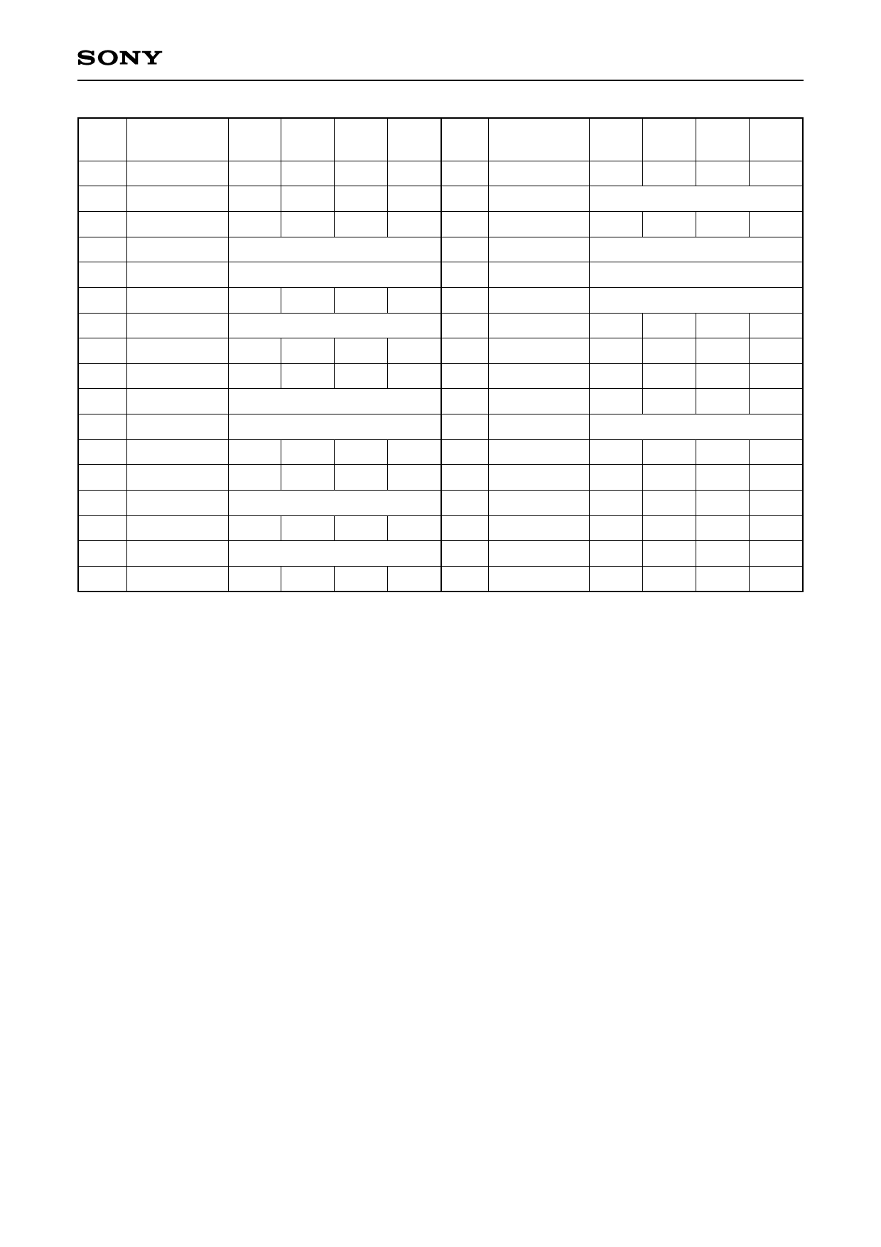
CXD3412GA
Pin
No.
Symbol
J9 H2
CAM SLP
STB
RST
Pin
No.
Symbol
ACT L
L ACT M2 VD∗1
CAM SLP STB RST
ACT L
L
H
K1 OSCO
ACT ACT ACT ACT M3 TEST1
—
K2 MCKO
ACT ACT L ACT M4 V2
ACT VM VM VM
K3 VDD5
—
M5 VH
—
K7 VDD2
—
M6 VL
—
K8 RG
ACT L
L ACT M7 TEST2
—
K9 VSS2
—
M8 RST
ACT ACT ACT L
L1 OSCI
ACT ACT ACT ACT M9 WEN
ACT L
L
L
L2 SSI1
L3 VSS4
ACT ACT ACT DIS
—
N1 SEN1
N2 HD∗1
ACT ACT ACT DIS
ACT L
L
H
L4 VM
—
N3 VSS6
—
L5 V1A
ACT VH VH VM N4 V4
ACT VM VM VL
L6 V3A
ACT VH VH VL N5 V1B
ACT VH VH VM
L7 VSS1
—
N6 V3B
ACT VH VH VL
L8 SSGSL
ACT ACT ACT ACT N7 SUB
ACT VH VH VL
L9 VDD1
—
N8 SNCSL
ACT ACT ACT ACT
M1 SCK1
ACT ACT ACT DIS N9 ID/EXP
ACT L
L
L
∗1 It is for output. For input, all items are "ACT".
Note) ACT means that the circuit is operating, and DIS means that loading is stopped.
L indicates a low output level, and H a high output level in the controlled status.
Also, VH, VM and VL indicate the voltage levels applied to VH (Pin M5), VM (Pin L3) and VL (Pin M6),
respectively, in the controlled status.
– 19 –
Share Link: 