ICX412_ データシートの表示(PDF) - Sony Semiconductor
部品番号
コンポーネント説明
メーカー
ICX412_ Datasheet PDF : 46 Pages
| |||
CXD3412GA
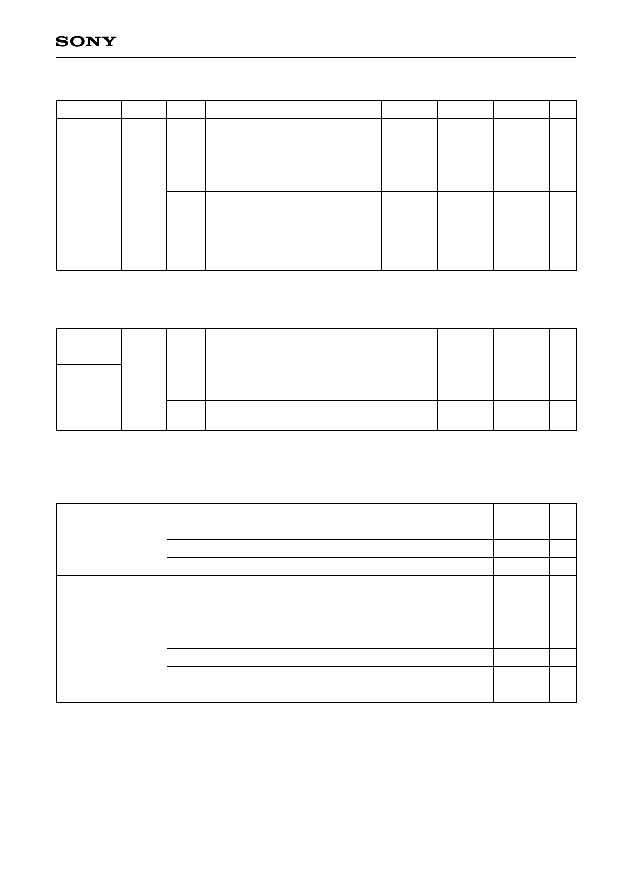
Inverter I/O Characteristics for Oscillation
(Within the recommended operating conditions)
Item
Logical Vth
Input
voltage
Output
voltage
Feedback
resistor
Oscillation
frequency
Pins Symbol
Conditions
Min.
OSCI LVth
VIH
OSCI
VIL
0.7VDDd
VOH
OSCO
VOL
Feed current where IOH = –3.6mA VDDd – 0.8
Pull-in current where IOL = 2.4mA
OSCI,
OSCO
RFB
VIN = VDDd or VSS
500k
OSCI,
OSCO
f
20
Typ.
VDDd/2
2M
Max. Unit
V
V
0.3VDDd V
V
0.4
V
5M
Ω
50 MHz
Inverter Input Characteristics for Base Oscillation Clock Duty Adjustment
(Within the recommended operating conditions)
Item
Logical Vth
Input
voltage
Input
amplitude
Pins
CKI
Symbol
LVth
VIH
VIL
Conditions
VIN fmax 50MHz sine wave
Min.
0.7VDDd
0.3
Typ.
VDDd/2
Max. Unit
V
V
0.3VDDd V
Vp-p
Note) Input voltage is the input voltage characteristics for direct input from an external source.
Input amplitude is the input amplitude characteristics in the case of input through a capacitor.
Switching Characteristics
(VH = 15.0V, VM = GND, VL = –7.5V)
Item
Symbol
Conditions
TTLM VL to VM
Rise time
TTMH VM to VH
TTLH VL to VH
TTML VM to VL
Fall time
TTHM VH to VM
TTHL VH to VL
VCLH
VCLL
Output noise voltage
VCMH
VCML
Min.
Typ.
Max. Unit
200
350
500 ns
200
350
500 ns
30
60
90
ns
200
350
500 ns
200
350
500 ns
30
60
90
ns
1.0
V
1.0
V
1.0
V
1.0
V
Notes)
1. The MOS structure of this IC has a low tolerance for static electricity, so full care should be given for
measures to prevent electrostatic discharge.
2. For noise and latch-up countermeasures, be sure to connect a by-pass capacitor (0.1µF or more) between
each power supply pin (VH, VL) and GND.
3. To protect the CCD image sensor, clamp the SUB pin output at VH before input to the CCD image sensor.
–8–
Share Link: 