AD5532-5 データシートの表示(PDF) - Analog Devices
部品番号
コンポーネント説明
メーカー
AD5532-5 Datasheet PDF : 20 Pages
| |||
AD5532
Table 7. Pin Function Descriptions
Pin
Function
AGND (1–2)
Analog GND pins.
AVCC (1–2)
Analog Supply pins. Voltage range from 4.75 V to 5.25 V.
VDD (1–4)
VDD Supply pins. Voltage range from 8 V to 16.5 V.
VSS (1–4)
VSS Supply pins. Voltage range from –4.75 V to –16.5 V.
DGND
Digital GND pins.
DVCC
Digital Supply pins. Voltage range from 2.7 V to 5.25 V.
DAC_GND (1–2) Reference GND supply for all DACs.
REF_IN
Reference voltage for Channels 0–31.
REF_OUT
Reference Output Voltage.
VOUT (0–31)
Analog Output Voltages from the 32 channels.
VIN
Analog Input Voltage. Connect this to AGND if operating in DAC mode only.
A4–A1, A0
Parallel Interface: 5 address pins for 32 channels. A4 = MSB of channel address. A0 = LSB. Internal pull-up devices on these
logic inputs. Therefore, they can be left floating and default to a logic high condition.
CAL
Parallel Interface: Control input that allows all 32 channels to acquire VIN simultaneously. Internal pull-down devices on
these logic inputs. Therefore, they can be left floating and default to a logic low condition
CS/SYNC
This is the active low Chip Select pin for the parallel interface and the Frame Synchronization pin for the serial interface.
WR
Parallel interface: Write pin; active low. This is used in conjunction with the CS pin to address the device using the parallel
interface. Internal pull-down devices on these logic inputs. Therefore, they can be left floating and default to a logic low
condition.
OFFSET_SEL
Parallel interface: Offset Select pin; active high. This is used to select the offset channel. Internal pull-down devices on
these logic inputs. Therefore, they can be left floating and default to a logic low condition
SCLK
Serial Clock Input for Serial Interface. This operates at clock speeds up to 14 MHz (20 MHz in ISHA mode).
DIN
Data Input for Serial Interface. Data must be valid on the falling edge of SCLK. Internal pull-up devices on these logic
inputs. Therefore, they can be left floating and default to a logic high condition.
DOUT
Output from the DAC registers for read back. Data is clocked out on the rising edge of SCLK and is valid on the falling
edge of SCLK.
SER/PAR
This pin allows the user to select whether the serial or parallel interface is used. If the pin is tied low, the parallel interface
is used. If it is tied high, the serial interface is used. Internal pull-down devices on these logic inputs. Therefore, they can
be left floating and default to a logic low condition.
OFFS_IN
Offset Input. The user can supply a voltage here to offset the output span. OFFS_OUT can also be tied to this pin if the
user wants to drive this pin with the offset channel.
OFFS_OUT
Offset Output. This is the acquired/programmed offset voltage which can be tied to OFFS_IN to offset the span.
BUSY
This output tells the user when the input voltage is being acquired. It goes low during acquisition and returns high when
the acquisition operation is complete.
TRACK/RESET
If this input is held high, VIN is acquired once the channel is addressed. While it is held low, the input to the gain/offset
stage is switched directly to VIN. The addressed channel begins to acquire VIN on the rising edge of TRACK. See TRACK
Input section for further information. This input can also be used as a means of resetting the complete device to its
power-on-reset conditions. This is achieved by applying a low-going pulse of between 90 ns and 200 ns to this pin. See
section on RESET Function for further details. Internal pull-up devices on these logic inputs. Therefore, they can be left
floating and default to a logic high condition.
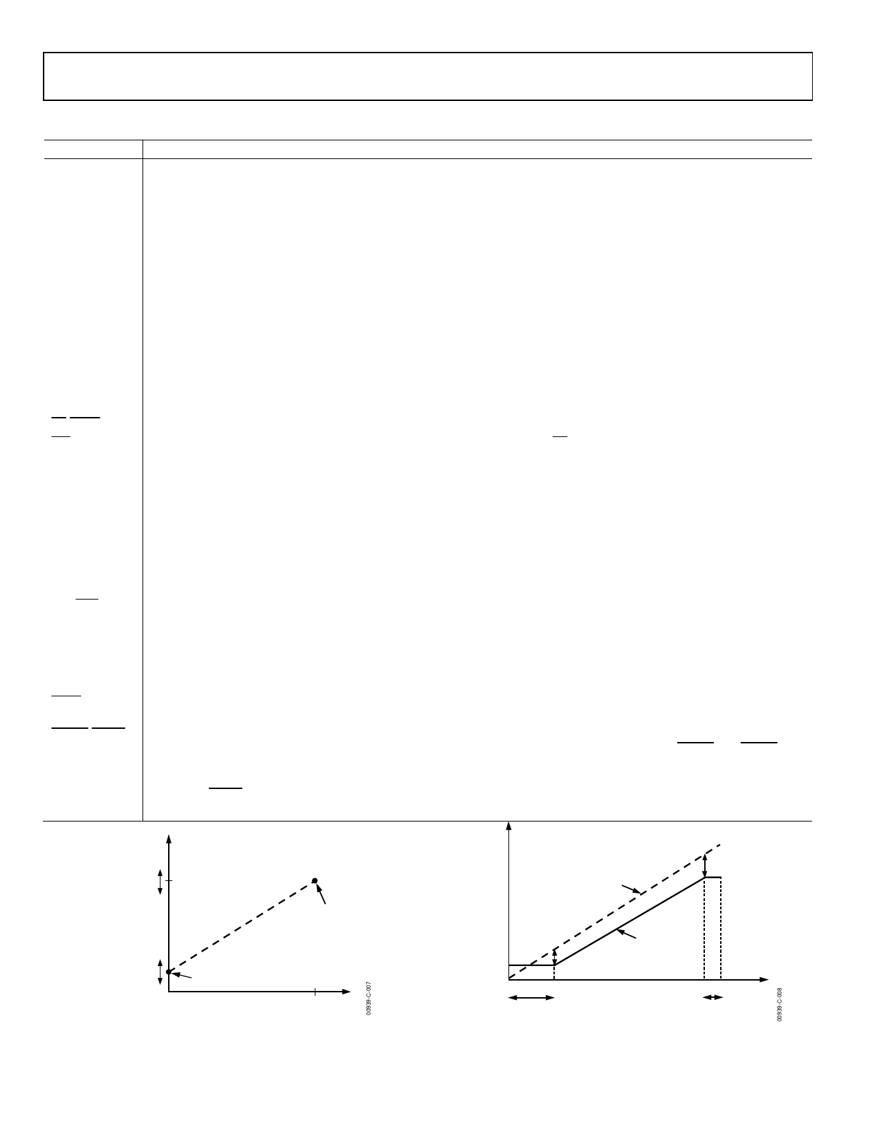
OUTPUT
VOLTAGE
FULL-SCALE
ERROR RANGE
IDEAL GAIN × REFIN
IDEAL TRANSFER
FUNCTION
VOUT
IDEAL
TRANSFER
FUNCTION
GAIN ERROR +
OFFSET ERROR
OFFSET
ERROR
ACTUAL
TRANSFER
FUNCTION
OFFSET
RANGE
IDEAL GAIN × 50mV
0
16k
DAC CODE
Figure 8. DAC Transfer Function (OFFS_IN=0)
0V
70mV
2.96 3V
VIN
LOWER
DEAD BAND
UPPER
DEAD BAND
Figure 9. ISHA Transfer Function
Rev. D | Page 10 of 20
Share Link: 