HV311LG データシートの表示(PDF) - Supertex Inc
部品番号
コンポーネント説明
メーカー
HV311LG Datasheet PDF : 21 Pages
| |||
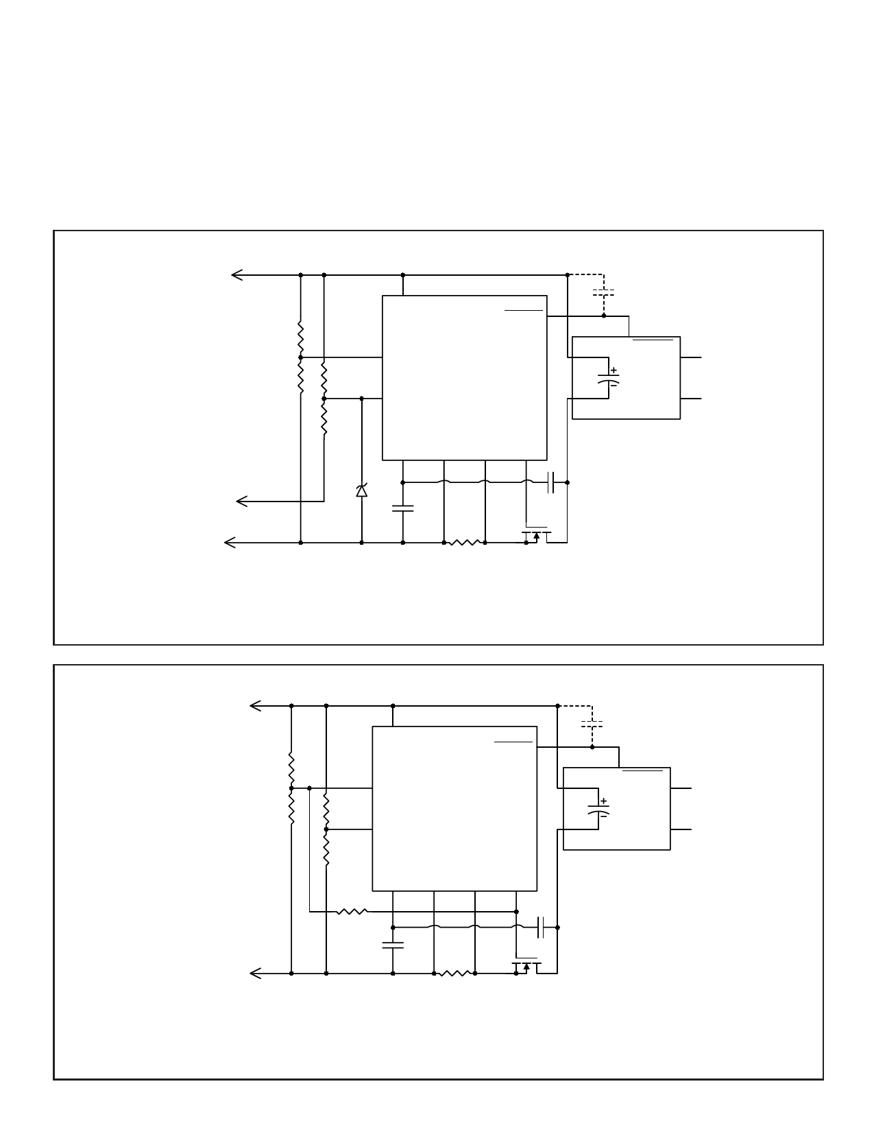
Application Information, cont’d.
If a system requires the use of a short connector pin on the
negative supply lead to guarantee that the power pins are fully
mated before the hotswap control circuit is enabled and uses
separate resistor dividers for UV and OV, then a 6.2V to 10V
zener diode must be connected from the OV pin to the VEE pin and
only the OV divider should be connected to the short pin
(Application Circuit 10).
HV301/HV311
Increasing Under Voltage Hysteresis
If the internally fixed under voltage hysteresis is insufficient for a
particular system application, then it may be increased by using
separate resistor dividers for OV and UV and providing a resistor
feedback path from the GATE pin to the UV pin (Application
Circuit 11).
Long
Pin
GND
R1
475kΩ
R2
16.2kΩ
-48V
Short
Pin
-48V
Long
Pin
8
VDD
PWRGD / PWRGD 1
R3
511kΩ
R4
10kΩ
3 UV
2 OV
HV301/
HV311
RAMP VEE
7
4
SENSE GATE
5
6
6.2V
C1
10nF
ENABLE / ENABLE +5V
Cload
DC/DC
PWM
COM
CONVERTER
R5
12.5mΩ
Q1
IRF530
Note: capacitor may be needed to slow PWRGD dv/dt if
oscillations are observed when VIN is close to OV.
Application Circuit 10
GND
R1
475kΩ
R2
16.2kΩ
-48V
8
VDD
PWRGD / PWRGD 1
3 UV
R3
511kΩ
2 OV
R4
10kΩ
HV301/
HV311
RAMP VEE SENSE GATE
7
4
5
6
R6
C1
10nF
ENABLE / ENABLE +5V
Cload
DC/DC
PWM
COM
CONVERTER
R5
12.5mΩ
Q1
IRF530
Note: capacitor may be needed to slow PWRGD dv/dt if
oscillations are observed when VIN is close to OV.
15
Application Circuit 11
Share Link: 