EN25P20 データシートの表示(PDF) - Eon Silicon Solution Inc.
部品番号
コンポーネント説明
メーカー
EN25P20 Datasheet PDF : 32 Pages
| |||
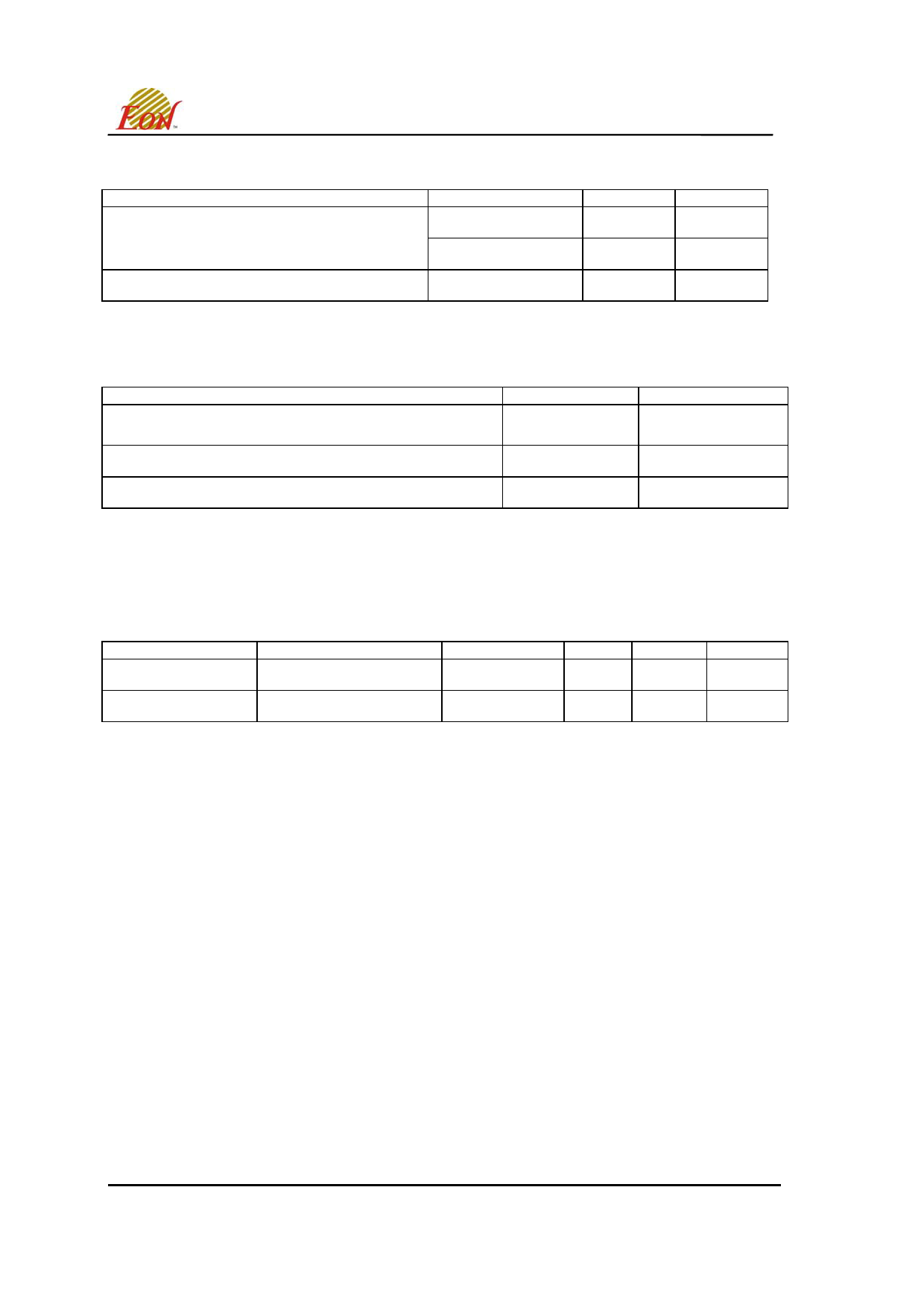
Table 13. DATA RETENTION and ENDURANCE
Parameter Description
Minimum Pattern Data Retention Time
Erase/Program Endurance
Test Conditions
150°C
125°C
-40 to 85 °C
EN25P20
Min
10
20
100k
Unit
Years
Years
cycles
Table 14. LATCH UP CHARACTERISTICS
Parameter Description
Input voltage with respect to Vss on all pins except I/O pins
(including A9, Reset and OE#)
Min
-1.0 V
Max
12.0 V
Input voltage with respect to Vss on all I/O Pins
-1.0 V
Vcc + 1.0 V
Vcc Current
-100 mA
100 mA
Note : These are latch up characteristics and the device should never be put under these conditions. Refer to
Absolute Maximum ratings for the actual operating limits.
Table 15. CAPACITANCE
( VCC = 2.7-3.6V)
Parameter Symbol
Parameter Description
Test Setup
Typ
Max
Unit
CIN
Input Capacitance
VIN = 0
6
pF
COUT
Output Capacitance
VOUT = 0
8
pF
Note : Sampled only, not 100% tested, at TA = 25°C and a frequency of 20MHz.
This Data Sheet may be revised by subsequent versions 27 ©2004 Eon Silicon Solution, Inc., www.essi.com.tw
or modifications due to changes in technical specifications.
Rev. D, Issue Date: 2007/05/07
Share Link: 