HA12160 データシートの表示(PDF) - Hitachi -> Renesas Electronics
部品番号
コンポーネント説明
メーカー
HA12160
Hitachi -> Renesas Electronics

HA12160 Datasheet PDF : 66 Pages
| |||
HA12163 Series
Application Note
1. Power Supply Range
HA12163 series are provided with four line output level, which will permit on optimum overload
margin for power supply conditions. And this series are designd to operate on single supply only.
In case of split supply use, please consult with sales engineer.
Table 1 Supply Voltage
Single supply
HA12163
6.5 V to 16.0 V
HA12164
7.2 V to 16.0 V
HA12165
8.5 V to 16.0 V
HA12160
8.2 V to 16.0 V
A. The lower limit of supply voltage depends on the line output reference level.
The minimum value of the overload margin is specified as 12 dB by Dolby Laboratories.
B. In the reverse-voltage conditions such as ‘D-GND is higher than VCC’ or ‘D-GND is lower than
GND’, excessive current flows into the D-GND to destory this IC. To prevent such destruction, pay
attention to the followings on using.
Short-circuit the D-GND and GND directory on the board mounting this IC.
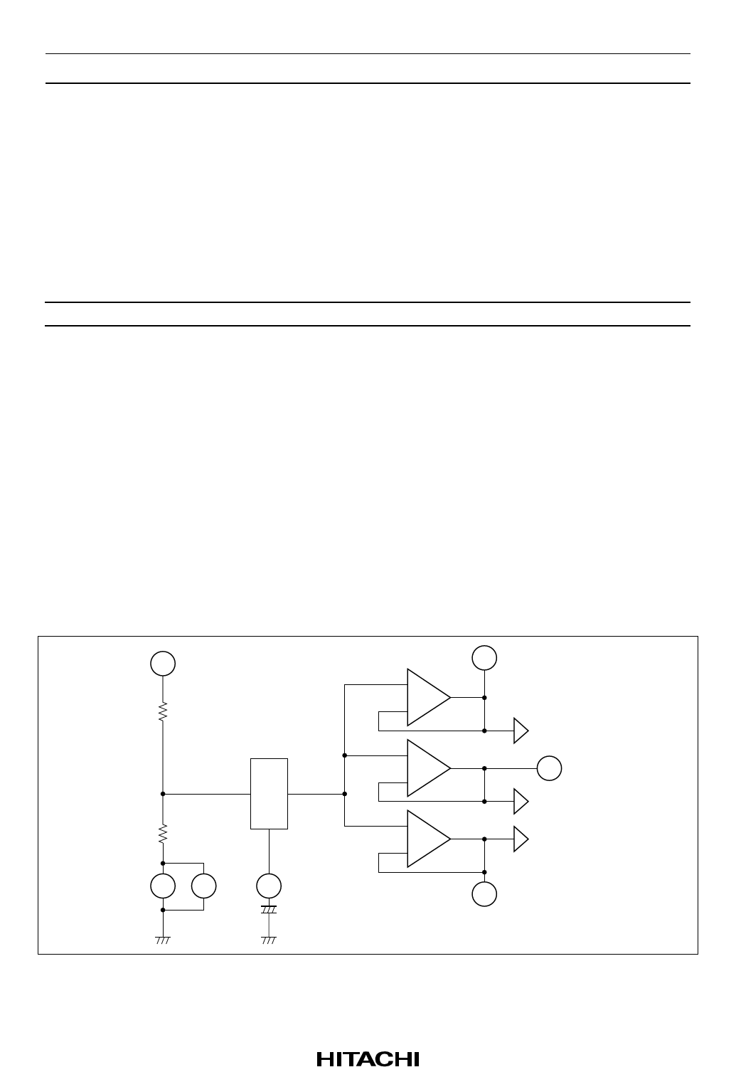
2. Reference Voltage
These devices provide the reference voltage of half the supply voltage that is the signal grounds. As the
peculiarity of these devices, the capacitor for the ripple filter is very small about 1/100 compared
with their usual value. The Reference voltage are provided for the left channel and the right channel
separately. The block diagram is shown as figure 1.
22 VCC
47 VREF(L)
+
–
L channel
reference
+
30 MS VREF
–
Music sensor
reference
+
R channel
–
reference
GND 49 50
40 RIP
+
C22
1µ
52 VREF(R)
Figure 1 The Block Diagram of Reference Voltage Supply
Rev.4, Jun. 1999, page 15 of 66
Share Link: