ICX232 データシートの表示(PDF) - Sony Semiconductor
部品番号
コンポーネント説明
メーカー
ICX232 Datasheet PDF : 49 Pages
| |||
CXD3410GA
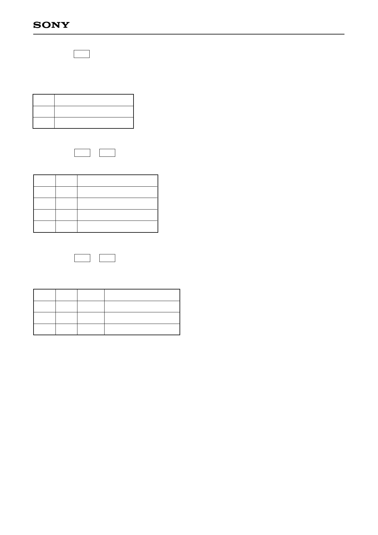
Control data: D12 CCD [CCD switching]
Specify CCD image sensor to use. However, the CCD switching bits are loaded to the CXD3410GA and reflected
at the falling edge of VD.
The default is "ICX224/ICX284".
D12
CCD
0 ICX224/ICX284
1 ICX202/ICX232
Control data: D36 to D37 LDAD [ADCLK logic phase]
This indicates the ADCLK logic phase adjustment data. The default is 90° relative to MCKO.
D37 D36
0
0
0
1
1
0
1
1
Degree of adjustment (°)
0
90
180
270
Control data: D38 to D39 STB [Standby]
The operating mode of the timing generator block is switched as follows. However, the standby bits are loaded
to the CXD3410GA and control is applied immediately at the rising edge of SEN1.
D39 D38 Symbol
Operating mode
X
0 CAM Normal operating mode
0
1
SLP Sleep mode
1
1
STB Standby mode
See the Pin Status Table for the pin status in each mode.
– 24 –
Share Link: 