ICX284 データシートの表示(PDF) - Sony Semiconductor
部品番号
コンポーネント説明
メーカー
ICX284 Datasheet PDF : 49 Pages
| |||
CXD3410GA
CCD Signal Processor Block Serial Interface Control
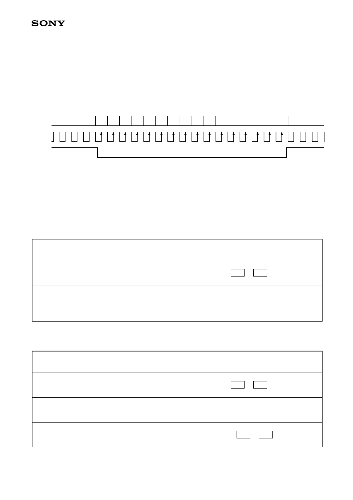
The CXD3410GA's CCD signal processor block basically loads the CCD signal processor block serial interface
data sent in the following format at the rising edge of SEN2, and the setting values are then reflected to the
operation 6 ADCLKI clocks after that.
CCD signal processor block serial interface control requires clock input to ADCLKI in order to load and reflect
the serial interface data to operation, so this should normally be performed when the timing generator block is
in the normal operation mode.
SSI2
SCK2
SEN2
00 01 02 03 04 05 06 07 08 09 10 11 12 13 14 15
There are four categories of CCD signal processor block serial interface data: standby control data, PGA gain
setting data, OB clamp level setting data, and input pulse polarity setting data.
Note that when data from multiple categories is loaded consecutively, the data for the category loaded last is
valid and data from other categories is lost. When transferring data from multiple categories, raise SEN2 for
each category and wait until the setting value 6 ADCKLI clocks after that has been reflected to operation, then
transmit the next category.
The detail of each data are described below.
Standby Control Data
Data
Symbol
D00 TEST
D01
to CTG
D03
D04
to FIXED
D14
D15 STB
Function
Test code
Category switching
—
Standby control
Data = 0
Set to 0.
Data = 1
D01 to D03 CTG
Set to All 0.
Normal operating mode Standby mode
PGA Gain Setting Data
Data
Symbol
D00 TEST
D01
to CTG
D03
D04
to FIXED
D05
D06
to GAIN
D15
Function
Test code
Category switching
—
PGA gain setting data
– 43 –
Data = 0
Set to 0.
Data = 1
D01 to D03 CTG
Set to All 0.
See D06 to D15 GAIN.
Share Link: 