SAA7205 データシートの表示(PDF) - Philips Electronics
部品番号
コンポーネント説明
メーカー
SAA7205 Datasheet PDF : 84 Pages
| |||
Philips Semiconductors
MPEG-2 systems demultiplexer
Preliminary specification
SAA7205H
The set of references can be generated either in master
(internal), or in slave (external) mode. Both options are
compared in Fig.12. If bit ‘v_in_pol’ (address 0x050A,
see Table 13) is programmed to logic 1, the sync
generator synchronizes to a rising edge on VIN, or it locks
to a falling edge. The sync circuitry automatically operates
in slave mode, if an appropriate edge occurs on VIN.
The position in the CCIR 601 field at a VIN triggering edge
is determined by the programmable registers ‘horiz_offset’
and ‘verti_offset’ (addresses 0x050F and 0x0510,
see Table 13). The phase relationships between the
COMSYNC and the HSYNC and VSYNV are
programmable (words: ‘h_sync_fall’, ‘h_sync_rise’,
‘v_sync_fall’, ‘v_sync_rise’, addresses 0x050B to 0x050E,
see Table 13). For details on the sync signal constellation
see Fig.13. It should be noted that the sync generator is
not reset by ‘Pwr_On_Rst’.
In the slave mode, the demultiplexer offers a possibility to
lock the 27 MHz system clock to the incoming vertical sync
pulses (VIN). The demultiplexer stores the position of the
horizontal and vertical sync counters as soon as a
triggering edge occurs on VIN (‘vin_hpos’, ‘vin_vpos’,
addresses 0x0408 and 0x0409, see Table 13).
The triggering edge furthermore resets the H and V
counters. The microcontroller can retrieve the position
data and calculate the difference between the detected
position and the required position (horiz_offset,
verti_offset). From this the microcontroller is able to derive
VCO control values (see Section “Program clock reference
processing”). The 27 MHz system clock can thus be
locked to external display sync sources.
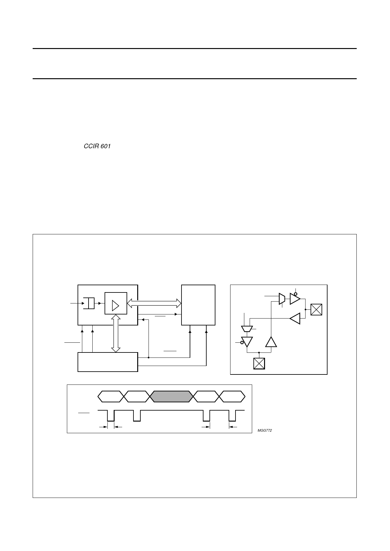
handbook, full pagewidth DMUX
TS
FIFO
MUX
VO7 to VO0
video/control
CLKP
CSDEM
control
VSEL
MDAT7
to
MDAT0
MICROCONTROLLER
CSVID
address
VIDEO
(THIRD
PARTY)
VSEL = 1
VO7 to VO0
CLKP
tCLKOL
tCLKOH
1
video FIFO
output
VSEL
VO
1
VSEL
DATA
MUX
MGG772
Fig.10 Merger of video elementary stream and video control data within the demultiplexer.
1997 Jan 21
21
Share Link: 