LA7209V データシートの表示(PDF) - SANYO -> Panasonic
部品番号
コンポーネント説明
メーカー
LA7209V Datasheet PDF : 14 Pages
| |||
Continued from preceding page.
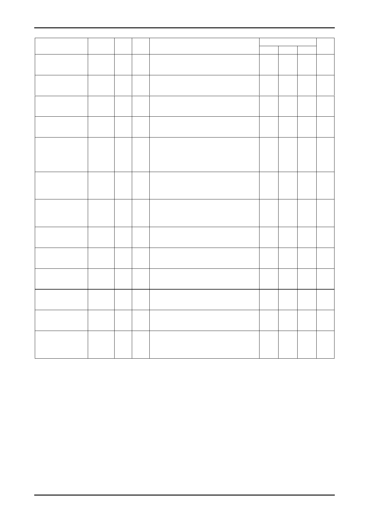
Parameter
Symbol
DET demodulation
sensitivity type A
DETA
DET demodulation
sensitivity type C
DETC
DET demodulation
sensitivity 423k
DT423
Comparator sensitivity
SCMP
Comparator output
“Low“
VCMPL
EVR characteristics 1
GEVR1
EVR characteristics 2
GEVR2
TAG DET output
VTAG
TAG DET output “Low“ VTAGL
Type Switch ON voltage TYPON
Type Switch OFF
voltage
TYPOF
Power save ON voltage PSON
Power save OFF voltage PSOFF
LA7209V
IN
T22
T23
T22
T23
T22
T23
T16A
T2A
T3A
T7
T22
T23
T22
T23
T22
T23
T22
T23
T11
T11
T12
T12
OUT
T18
T18
T18
T15
T15
T18
T18
T10
T10
T4
T4
T20
T20
Conditions
VIN = 5.0Vp-p (13.5MHz)+28mVp-p (847kHz)
Measure the C/N ratio of the 847kHz component.
SW1 : 1, SW2 : 2, SW3 : 2, SW4 : 1, SW5 : 1, SW6 : 2
VIN = 5.0Vp-p (13.5MHz)+28mVp-p (106kHz)
Measure the C/N ratio of the 106kHz component.
SW1 : 2, SW2 : 2, SW3 : 2, SW4 : 1, SW5 : 1, SW6 : 2
VIN = 5.0Vp-p (13.5MHz)+28mVp-p (423kHz)
Measure the C/N ratio of the 423kHz component.
SW1 : 2, SW2 : 2, SW3 : 2, SW4 : 1, SW5 : 1, SW6 : 2
VIN = 10mVp-p, 106kHz, Square wave
Measure the amplitude of output waveform.
SW1 : 2, SW2 : 2, SW3 : 2, SW4 : 1, SW5 : 2, SW6 : 2
VIN = 3.0Vp-p, 106kHz, Square wave (T7)
VIN = 3.0Vp-p, 13.5MHz, Square wave (T2A/T3A :
Opposite)
Measure the bottom of DC of output waveform.
SW1 : 2, SW2 : 2, SW3 : 2, SW4 : 1, SW5 : 2, SW6 : 2
VIN = 5.0Vp-p (13.5MHz)+28mVp-p (847kHz)
Measure the output level at Pin 18, Calculate
output/input ratio.
SW1 : 2, SW2 : 2, SW3 : 2, SW4 : 1, SW5 : 1, SW6 : 2
VIN = 5.0Vp-p (13.5MHz)+28mVp-p (847kHz)
Measure the output level at Pin 18,
Calculate GEVR1 minus output level.
SW1 : 2, SW2 : 2, SW3 : 2, SW4 : 1, SW5 : 2, SW6 : 2
VIN = 5.0Vp-p (13.5MHz)+28mVp-p (847kHz)
Measure the output level at Pin 18.
SW1 : 2, SW2 : 2, SW3 : 2, SW4 : 1, SW5 : 1, SW6 : 2
VIN = 5.0Vp-p (13.5MHz)+28mVp-p (847kHz)
Measure the DC bottom level of output wave at Pin 18.
SW1 : 2, SW2 : 2, SW3 : 2, SW4 : 1, SW5 : 1, SW6 : 2
DC voltage that T4 sinks.
SW1 : Open, SW2 : 2, SW3 : 3, SW4 : 2, SW5 : 2,
SW6 : 2
DC voltage that T4 opens.
SW1 : Open, SW2 : 2, SW3 : 3, SW4 : 2, SW5 : 2,
SW6 : 2
DC voltage that DC current 1mA or less flows into T20.
SW1 : 2, SW2 : Open, SW3 : 3, SW4 : 2, SW5 : 2,
SW6 : 2
DC voltage that DC current 10mA or more flows into
T20.
SW1 : 2, SW2 : Open, SW3 : 3, SW4 : 2, SW5 : 2,
SW6 : 2
Ratings
min
typ
42
45
47
50
45
48
2.5
3.0
0
0.2
24
30
14
16
2.5
3.0
0
0.2
0.0
1.7
1.7
0.0
max
48
53
51
3.1
0.4
18
3.1
0.4
1.3
5.0
5.0
1.3
Unit
dB
dB
dB
Vp-p
V
dB
dB
Vp-p
V
V
V
V
V
No.A0641-3/14
Share Link: 