LT3579E(RevA) データシートの表示(PDF) - Linear Technology
部品番号
コンポーネント説明
メーカー
LT3579E Datasheet PDF : 42 Pages
| |||
LT3579/LT3579-1
APPLICATIONS INFORMATION
BOOST CONVERTER COMPONENT SELECTION
VIN
5V
L1
2.2µH
D1
30V, 4A
COUT1
OPTIONAL
M1
VOUT
12V
1.7A
10µF
RFB
SW1 SW2
130k
VIN
100k
FAULT
FB
GATE
RGATE
6.3k
COUT
10µF
VIN
200k
CIN
22µF
LT3579
SHDN
CLKOUT
RT
VC
SYNC GND SS
RT
86.6k
CSS
0.1µF
CF
47pF
RC
8k
CC
2.2nF
35791 F06
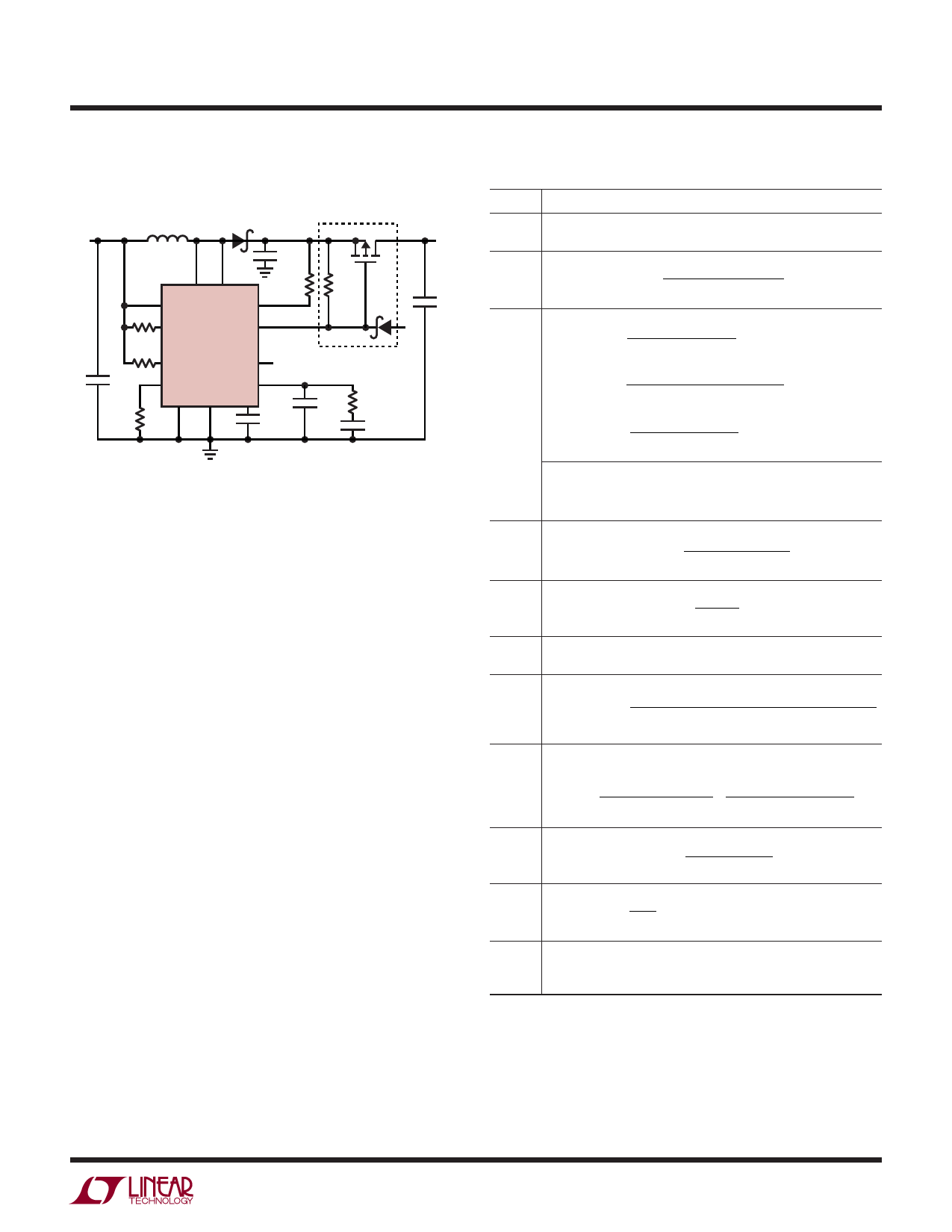
Figure 6. Boost Converter – The Component Values Given Are
Typical Values for a 1MHz, 5V to 12V Boost
The LT3579 can be configured as a Boost converter as in
Figure 6. This topology allows for positive output voltages
that are higher than the input voltage. An external PMOS
(optional) driven by the GATE pin of the LT3579 can achieve
input or output disconnect during a FAULT event. A single
feedback resistor sets the output voltage. For output
voltages higher than 40V, see the Charge Pump topology
in the Charge Pump Aided Regulators section.
Table 1 is a step-by-step set of equations to calculate
component values for the LT3579 when operating as a
Boost converter. Input parameters are input and output
voltage, and switching frequency (VIN, VOUT and fOSC
respectively). Refer to the Appendix for further information
on the design equations presented in Table 1.
Variable Definitions:
VIN = Input Voltage
VOUT = Output Voltage
DC = Power Switch Duty Cycle
fOSC = Switching Frequency
IOUT = Maximum Output Current
IRIPPLE = Inductor Ripple Current
RDSON_PMOS = RDSON of External PMOS (set to 0 if not
using PMOS)
Table 1. Boost Design Equations
PARAMETERS/EQUATIONS
Step 1: Pick VIN, VOUT, and fOSC to calculate equations below.
Inputs
Step 2:
DC
DC ≅ VOUT – VIN + 0.5V
VOUT + 0.5V – 0.27V
Step 3:
L1
Step 4:
IRIPPLE
( ) LTYP =
VIN – 0.27V • DC
fOSC • 1.8A
(1)
LMIN
=
( VIN
– 0.27V) • (2 • DC –
4A • fOSC • (1 – DC)
1)
(2)
( ) LMAX =
VIN – 0.27V • DC
fOSC • 0.5A
(3)
• Solve equations 1, 2, and 3 for a range of L1 values.
• The minimum of the L1 value range is the higher of LTYP
and LMIN.
• The maximum of the L1 value range is LMAX.
( ) IRIPPLE =
VIN – 0.27V • DC
fOSC • L1
Step 5:
IOUT
( ) IOUT
=
6A
–
IRIPPLE
2
•
1 – DC
Step 6:
D1
VR > VOUT ; IAVG > IOUT
Step 7:
COUT,
COUT1
( ) COUT =COUT1 = fOSC •
IOUT • DC
0.01•VOUT –0.5•IOUT
• RDSON_PMOS
Step 8:
CIN
Step 9:
RFB
CIN = CPWR + CVIN
CIN
=
8
•
IRIPPLE
fOSC • 0.005
•
VIN
+
40
•
6A • DC
fOSC • 0.005
•
VIN
RFB
=
VOUT – 1.215V
83.3µA
Step 10:
RT
RT
=
87.6
fOSC
– 1;
fOSC
in MHz
and RT
in kΩ
Step 11:
PMOS
Only needed for input or output disconnect. See PMOS
Selection in the Appendix for information on sizing the PMOS
and the biasing resistor, RGATE.
Note: The maximum design target for peak switch current is 6A and
is used in this table. The final values for COUT and CIN may deviate
from the above equations in order to obtain desired load transient
performance for a particular application.
For more information www.linear.com/LT3579
35791fa
13
Share Link: 