LT3579IUFD-1-PBF データシートの表示(PDF) - Linear Technology
部品番号
コンポーネント説明
メーカー
LT3579IUFD-1-PBF Datasheet PDF : 40 Pages
| |||
LT3579/LT3579-1
APPLICATIONS INFORMATION
Clock Synchronization
An external source can set the operating frequency of the
LT3579 by providing a digital clock signal into the SYNC
pin (RT resistor still required). The LT3579 will operate at
the SYNC clock frequency. The LT3579 will revert to its
internal free-running oscillator clock when the SYNC pin is
driven below 0.4V for a few free-running clock periods.
Driving SYNC high for an extended period of time
effectively stops the operating clock and prevents latch
SR1 from becoming set (see Block Diagram). As a result,
the switching operation of the LT3579 will stop and the
CLKOUT pin will be held at ground.
The duty cycle of the SYNC signal must be between 20%
and 80% for proper operation. Also, the frequency of the
SYNC signal must meet the following two criteria:
1. SYNC may not toggle outside the frequency
range of 200kHz-2.5MHz unless it is stopped
below 0.4V to enable the free-running oscillator.
2. The SYNC frequency can always be higher than
the free-running oscillator frequency (as set by the
RT resistor), fOSC, but should not be less than 25%
below fOSC.
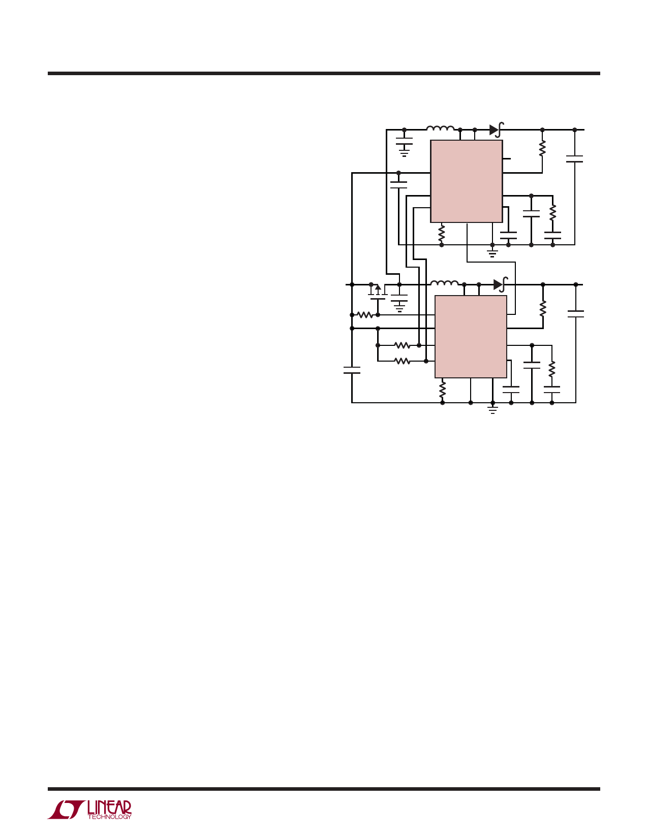
CLOCK SYNCHRONIZATION OF ADDITIONAL
REGULATORS
The CLKOUT pin of the LT3579 can synchronize additional
switching regulators and/or additional LT3579s as shown
in Figure 12.
The frequency of the master LT3579 is set by the external
RT resistor. The SYNC pin of the slave LT3579 is driven
by the CLKOUT pin of the master LT3579. Note that the
RT pin of the slave LT3579 must have a resistor tied to
ground. It takes a few clock cycles for the CLKOUT signal
to begin oscillating, and it’s preferable for all LT3579s to
have the same internal free-running frequency. Therefore,
in general, use the same value RT resistor for all of the
synchronized LT3579s.
3.3μH
10μF
SW1 SW2
GATE
CLKOUT
VIN LT3579 FB
4.7μF
SLAVE
FAULT
VC
SHDN
SS
RT SYNC GND
86.6k
200k
68pF
8k
0.1μF
3.3nF
VOUT
18V
1A
10μF
s2
VIN
5V
10k
4.7μF
10μF
100k
110k
2.2μH
SW1 SW2
GATE
CLKOUT
VIN LT3579 FB
MASTER
FAULT
VC
SHDN
SS
RT SYNC GND
86.6k
130k
47pF
0.1μF
8k
2.2nF
VOUT
12V
1.7A
10μF
s3
3579 F12
Figure 12. Synchronize Multiple LT3579s. The External PMOS
Disconnects the Input from Both Power Paths During FAULT Events
Also, the FAULT pins can be tied together so that a fault
condition from one LT3579 causes all of the LT3579s to
enter fault, until the fault condition disappears.
2-Phase Converters using LT3579-1
The CLKOUT pin on the LT3579-1 is ~180° out of phase
with the internal oscillator, which allows two LT3579-1s to
operate in parallel for a high current, high power output.
The advantage of multiphase converters is that the ripple
current flowing into the output node is divided by the
number of phases or ICs used to generate the output
voltage. The VIN, SHDN, FAULT, FB, and VC pins of all the
LT3579-1s should be connected together. Figure 13 shows
a typical application of a 2-phase 12V to 24V boost with
output disconnect.
35791f
21
Share Link: 