LT3581IDE-TRPBF データシートの表示(PDF) - Linear Technology
部品番号
コンポーネント説明
メーカー
LT3581IDE-TRPBF Datasheet PDF : 36 Pages
| |||
LT3581
APPLICATIONS INFORMATION
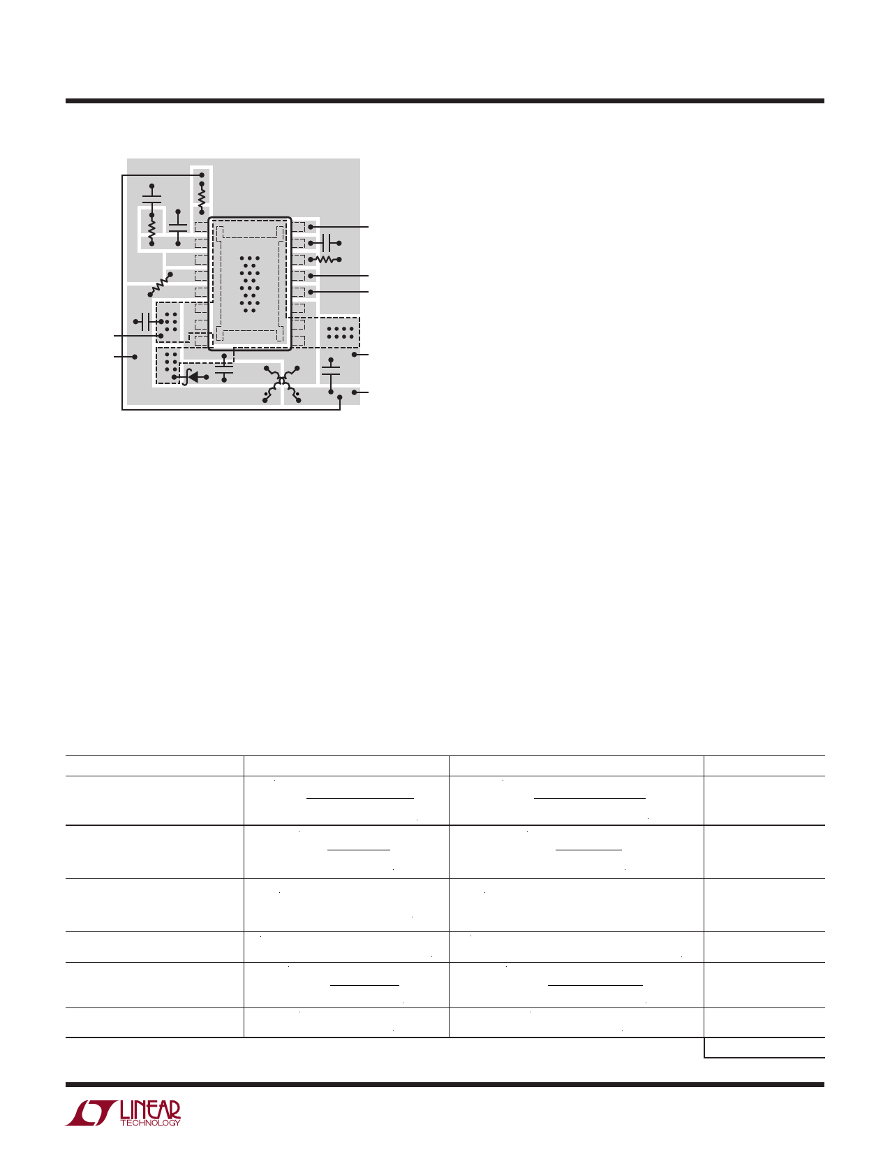
GND
1
16
SYNC
2
17
15
3
14
4
13
SHDN
CIN
–
VIN
+
5
6
A
7
8
C
C1
12
11
10
B
9
CLKOUT
GND
COUT
D1
L1
• L2
– VOUT
3581 F10
A: RETURN CIN GROUND DIRECTLY TO LT3581 EXPOSED PAD PIN 17. IT IS ADVISED
TO NOT COMBINE CIN GROUND WITH GND EXCEPT AT THE EXPOSED PAD.
B: RETURN COUT GROUND DIRECTLY TO LT3581 EXPOSED PAD PIN 17. IT IS ADVISED
TO NOT COMBINE COUT GROUND WITH GND EXCEPT AT THE EXPOSED PAD.
C: RETURN D1 GROUND DIRECTLY TO LT3581 EXPOSED PAD PIN 17. IT IS ADVISED
TO NOT COMBINE D1 GROUND WITH GND EXCEPT AT THE EXPOSED PAD.
L1, L2: MOST COUPLED INDUCTOR MANUFACTURERS USE CROSS PINOUT FOR
IMPROVED PERFORMANCE.
Figure 10. Suggested Component Placement for Dual Inductor
Inverting Topology (MSOP Shown, DFN Similar, Not to Scale.)
Pin 15 on DFN or Pin 17 on MSOP Is the Exposed Pad Which
Must Be Soldered Directly to the Local Ground Plane for
Adequate Thermal Performance. Multiple Vias to Additional
Ground Planes Will Improve Thermal Performance
THERMAL CONSIDERATIONS
Overview
For the LT3581 to deliver its full output power, it is imp
erative that a good thermal path be provided to dissipate
the heat generated within the package. This can be
accomplished by taking advantage of the thermal pad on
the underside of the IC. It is recommended that multiple
vias in the printed circuit board be used to conduct heat
away from the IC and into a copper plane with as much
area as possible.
Power and Thermal Calculations
Power dissipation in the LT3581 chip comes from four
primary sources: switch I2R losses, switch dynamic
losses, NPN base drive DC losses, and miscellaneous
input current losses. These formulas assume continuous
mode operation, so they should not be used for calculating
thermal losses or efficiency in discontinuous mode or at
light load currents.
The following example calculates the power dissipa-
tion in the LT3581 for a particular boost application
(VIN = 5V, VOUT = 12V, IOUT = 0.83A, fOSC = 2MHz, VD = 0.45V,
VCESAT = 0.21V).
To calculate die junction temperature, use the appropriate
thermal resistance number and add in worst-case ambient
temperature:
TJ = TA + θJA • PTOTAL
Table 4. Power Calculations Example for Boost Converter with VIN = 5V, VOUT = 12V, IOUT = 0.83A, fOSC = 2MHz, VD = 0.45V, VCESAT = 0.21V
DEFINITION OF VARIABLES
EQUATIONS
DESIGN EXAMPLE
VALUE
DC = SWITCH DUTY CYCLE
DC = VOUT – VIN + VD
VOUT + VD – VCESAT
DC = 12V – 5V + 0.45V
12V + 0.45V – 0.21V
DC = 60.9%
IIN = Average Switch Current
η = Power Conversion Efficiency
(typically 88% at high currents)
PSWDC = Switch I2R Loss (DC)
RSW = Switch Resistance (typically
90mΩ combined SW1 and SW2)
PSWAC = Switch Dynamic Loss (AC)
IIN
=
VOUT • IOUT
VIN • η
PSWDC = DC • IIN2 • RSW
PSWAC = 13ns • IIN • VOUT • fOSC
IIN
=
12V
5V
• 0.83A
• 0.88
PSWDC = 0.609 • (2.3A)2 • 90mΩ
PSWAC = (13ns) • 2.3A • 12V • (2MHz)
IIN = 2.3A
PSWDC = 290mW
PSWAC = 718mW
PBDC = Base Drive Loss (DC)
PBDC
=
VIN
• IIN
45
• DC
PBDC
=
5V
•2.3A •
45
0.609
PBDC = 156mW
PINP = Input Power Loss
PINP = 9mA • VIN
PINP = 9mA • 5V
PINP = 45mW
PTOTAL = 1.209W
3581fb
For more information www.linear.com/LT3581
17
Share Link: 